EVAL6730 STMicroelectronics, EVAL6730 Datasheet - Page 6
EVAL6730
Manufacturer Part Number
EVAL6730
Description
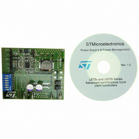
EVAL BOARD FOR L6730XX
Manufacturer
STMicroelectronics
Type
Motor / Motion Controllers & Driversr
Datasheets
1.L6730TR.pdf
(52 pages)
2.L6730DTR.pdf
(50 pages)
3.EVAL6730.pdf
(9 pages)
4.EVAL6732.pdf
(43 pages)
Specifications of EVAL6730
Main Purpose
DC/DC, Step Down
Outputs And Type
1, Non-Isolated
Power - Output
66W
Voltage - Output
3.3V
Current - Output
20A
Voltage - Input
4.5 ~ 14V
Regulator Topology
Buck
Frequency - Switching
400kHz
Board Type
Fully Populated
Utilized Ic / Part
L6730
Input Voltage
8 V to 52 V
Product
Power Management Modules
Lead Free Status / RoHS Status
Lead free / RoHS Compliant
For Use With/related Products
L6208
Other names
497-5501
Available stocks
Company
Part Number
Manufacturer
Quantity
Price


AN1451 APPLICATION NOTE
For Example, if a maximum ripple of 500mV is allowed and I
Actually, current sunk by V
charge of internal freewheeling diodes. Duration of these peaks is, tough, very short, and can be filtered using
a small value (100÷200 nF), good quality ceramic capacitor, connected as close as possible to the V
and GND pins of the IC. Bulk capacitor will be chosen with maximum operating voltage 25% greater than the
maximum supply voltage, considering also power supply tolerances. For example, with a 48V nominal power
supply, with 5% tolerance, maximum voltage is 50.4V, then operating voltage for the capacitor should be at least
63V.
2.4 Layout Considerations
Working with devices that combine high power switches and control logic in the same IC, careful attention has
to be paid to the PCB layout. In extreme cases, Power DMOS commutation can induce noises that could cause
improper operation in the logic section of the device. Noise can be radiated by high dv/dt nodes or high di/dt
paths, or conducted through GND or Supply connections. Logic connections, especially high-impedance nodes
(actually all logic inputs, see further), must be kept far from switching nodes and paths. With the L6208, in par-
ticular, external components for the charge pump circuitry should be connected together through short paths,
since these components are subject to voltage and current switching at relatively high frequency (600kHz). Pri-
mary mean in minimizing conducted noise is working on a good GND layout (see Figure 5).
Figure 5. Typical Application and Layout suggestions.
6/43
Logic Supply
3.3 ÷ 5 V
+
-
Custom Logic
V
ref
µC
or
= 0 ÷1V
SA
and V
R1
ESR
ESR
C1
SB
CW / CCW
CONTROL
RESET
HALF / FULL
CLOCK
EN
V
OUT
pins of the device is subject to higher peaks due to reverse recovery
refA
C2
0.5 V
------------
2 · I
1
-- -
2
2A
1A
I
OUT
OUT
V
refB
2A
0.5 V
------------
R2
OUT
OUT
2A
=
1B
· ESR in slow decay
OUT
RC
A
· ESR in fast decay
250m
2B
C3
=
Stepper Motor
L6208
2-Phase
V
1 25m
BOOT
R3
D1
C5
R4
RC
in slow decay, and
B
CP
OUT
C4
GND
D2
in fast decay.
= 2A, the capacitor ESR should be lower than:
GND
V
SA
GND
SENSE
SENSE
V
SB
GND
A
B
C8
R5
R6
C6
C7
V
S
+
= 8 ÷ 52 V
-
SA
, V
SB
Related parts for EVAL6730
Image
Part Number
Description
Manufacturer
Datasheet
Request
R

Part Number:
Description:
STMicroelectronics [RIPPLE-CARRY BINARY COUNTER/DIVIDERS]
Manufacturer:
STMicroelectronics
Datasheet:
Part Number:
Description:
STMicroelectronics [LIQUID-CRYSTAL DISPLAY DRIVERS]
Manufacturer:
STMicroelectronics
Datasheet:

Part Number:
Description:
BOARD EVAL FOR MEMS SENSORS
Manufacturer:
STMicroelectronics
Datasheet:
Part Number:
Description:
NPN TRANSISTOR POWER MODULE
Manufacturer:
STMicroelectronics
Datasheet:
Part Number:
Description:
TURBOSWITCH ULTRA-FAST HIGH VOLTAGE DIODE
Manufacturer:
STMicroelectronics
Datasheet:
Part Number:
Description:
Manufacturer:
STMicroelectronics
Datasheet:
Part Number:
Description:
DIODE / SCR MODULE
Manufacturer:
STMicroelectronics
Datasheet:
Part Number:
Description:
DIODE / SCR MODULE
Manufacturer:
STMicroelectronics
Datasheet:
Part Number:
Description:
Search -----> STE16N100
Manufacturer:
STMicroelectronics
Datasheet:
Part Number:
Description:
Search ---> STE53NA50
Manufacturer:
STMicroelectronics
Datasheet:
Part Number:
Description:
NPN Transistor Power Module
Manufacturer:
STMicroelectronics
Datasheet:
Part Number:
Description:
DIODE / SCR MODULE
Manufacturer:
STMicroelectronics
Datasheet: