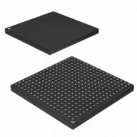
AT91SAM9G45-CU Atmel, AT91SAM9G45-CU Datasheet - Page 24

AT91SAM9G45-CU
Manufacturer Part Number
AT91SAM9G45-CU
Description
MCU ARM9 324-TFBGA
Manufacturer
Atmel
Series
AT91SAMr
Datasheets
1.AT91SAM9G45-EKES.pdf
(56 pages)
2.AT91SAM9G45-EKES.pdf
(1218 pages)
3.AT91SAM9G45-CU.pdf
(10 pages)
Specifications of AT91SAM9G45-CU
Core Processor
ARM9
Core Size
16/32-Bit
Speed
400MHz
Connectivity
EBI/EMI, Ethernet, I²C, IrDA, MMC, SPI, SSC, UART/USART, USB
Peripherals
AC'97, DMA, I²S, LCD, POR, PWM, WDT
Number Of I /o
160
Program Memory Size
64KB (64K x 8)
Program Memory Type
ROM
Ram Size
128K x 8
Voltage - Supply (vcc/vdd)
0.9 V ~ 1.1 V
Data Converters
A/D 8x10b
Oscillator Type
Internal
Operating Temperature
-40°C ~ 85°C
Package / Case
324-TFBGA
Processor Series
AT91SAMx
Core
ARM926EJ-S
Data Bus Width
32 bit
Data Ram Size
64 KB
Interface Type
I2C, SPI, UART
Maximum Clock Frequency
800 MHz
Number Of Programmable I/os
160
Number Of Timers
5
Maximum Operating Temperature
+ 85 C
Mounting Style
SMD/SMT
3rd Party Development Tools
JTRACE-ARM-2M, MDK-ARM, RL-ARM, ULINK2
Development Tools By Supplier
AT91SAM-ICE, AT91-ISP
Minimum Operating Temperature
- 40 C
On-chip Adc
10 bit
Controller Family/series
AT91
No. Of I/o's
160
Ram Memory Size
64KB
Cpu Speed
400MHz
No. Of Timers
2
Rohs Compliant
Yes
For Use With
AT91SAM9G45-EKES - KIT EVAL FOR AT91SAM9G45
Lead Free Status / RoHS Status
Lead free / RoHS Compliant
Eeprom Size
-
Lead Free Status / Rohs Status
Lead free / RoHS Compliant
Available stocks
Company
Part Number
Manufacturer
Quantity
Price
Company:
Part Number:
AT91SAM9G45-CU
Manufacturer:
ATMEL
Quantity:
1 000
Company:
Part Number:
AT91SAM9G45-CU
Manufacturer:
Atmel
Quantity:
31
Part Number:
AT91SAM9G45-CU
Manufacturer:
ATMEL/爱特梅尔
Quantity:
20 000
7.1
7.2
7.2.1
24
Memory Mapping
Embedded Memories
AT91SAM9G45
Internal SRAM
A first level of address decoding is performed by the AHB Bus Matrix, i.e., the implementation of
the Advanced High performance Bus (AHB) for its Master and Slave interfaces with additional
features.
Decoding breaks up the 4 Gbytes of address space into 16 banks of 256 Mbytes. The banks 1 to
6 are directed to the EBI that associates these banks to the external chip selects NCS0 to
NCS5.
The bank 7 is directed to the DDRSDRC0 that associates this bank to DDR_NCS chip select
and so dedicated to the 4-port DDR2/ LPDDR controller.
The bank 0 is reserved for the addressing of the internal memories, and a second level of
decoding provides 1 Mbyte of internal memory area. The bank 15 is reserved for the peripherals
and provides access to the Advanced Peripheral Bus (APB).
Other areas are unused and performing an access within them provides an abort to the master
requesting such an access.
The AT91SAM9G45 product embeds a total of 64 Kbytes high-speed SRAM split in 4 blocks of
16 KBytes connected to one slave of the matrix. After reset and until the Remap Command is
performed, the four SRAM blocks are contiguous and only accessible at address 0x00300000.
After Remap, the SRAM also becomes available at address 0x0.
Figure 7-2.
The AT91SAM9G45 device embeds two memory features. The processor Tightly Coupled Mem-
ory Interface (TCM) that allows the processor to access the memory up to processor speed
(PCK) and the interface on the AHB side allowing masters to access the memory at AHB speed
(MCK).
A wait state is necessary to access the TCM at 400 MHz. Setting the bit NWS_TCM in the bus
Matrix TCM Configuration Register of the matrix inserts a wait state on the ITCM and DTCM
accesses.
0x00300000
Internal SRAM Reset
RAM
64K
Remap
RAM
64K
6438ES–ATARM–21-Jun-10
0x00000000


