MC68HC908GR4CFAE Freescale Semiconductor, MC68HC908GR4CFAE Datasheet - Page 306
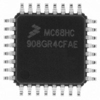
MC68HC908GR4CFAE
Manufacturer Part Number
MC68HC908GR4CFAE
Description
IC MCU 4K FLASH 8.2MHZ 32-LQFP
Manufacturer
Freescale Semiconductor
Series
HC08r
Specifications of MC68HC908GR4CFAE
Core Processor
HC08
Core Size
8-Bit
Speed
8MHz
Connectivity
SCI, SPI
Peripherals
LVD, POR, PWM
Number Of I /o
21
Program Memory Size
4KB (4K x 8)
Program Memory Type
FLASH
Ram Size
384 x 8
Voltage - Supply (vcc/vdd)
2.7 V ~ 5.5 V
Data Converters
A/D 6x8b
Oscillator Type
Internal
Operating Temperature
-40°C ~ 85°C
Package / Case
32-LQFP
Controller Family/series
HC08
No. Of I/o's
21
Ram Memory Size
1KB
Cpu Speed
8MHz
No. Of Timers
1
Embedded Interface Type
I2C, SCI, SPI
Rohs Compliant
Yes
Processor Series
HC08G
Core
HC08
Data Bus Width
8 bit
Data Ram Size
384 B
Interface Type
SCI, SPI
Maximum Clock Frequency
8 MHz
Number Of Programmable I/os
21
Number Of Timers
3
Operating Supply Voltage
3 V to 5 V
Maximum Operating Temperature
+ 125 C
Mounting Style
SMD/SMT
Development Tools By Supplier
FSICEBASE, DEMO908GZ60E, M68CBL05CE, M68EML08GPGTE
Minimum Operating Temperature
- 40 C
On-chip Adc
8 bit, 6 Channel
Lead Free Status / RoHS Status
Lead free / RoHS Compliant
Eeprom Size
-
Lead Free Status / Rohs Status
Details
Available stocks
Company
Part Number
Manufacturer
Quantity
Price
Company:

Part Number:
MC68HC908GR4CFAE
Manufacturer:
Freescale Semiconductor
Quantity:
10 000


Serial Peripheral Interface (SPI)
Technical Data
306
CAPTURE STROBE
FOR REFERENCE
SPSCK; CPOL = 0
SPSCK; CPOL =1
SPSCK CYCLE #
FROM MASTER
SS
FROM SLAVE
;
TO SLAVE
MOSI
MISO
Figure 20-6. Transmission Format (CPHA = 1)
out (MISO), and master out/slave in (MOSI) pins are directly connected
between the master and the slave. The MISO signal is the output from
the slave, and the MOSI signal is the output from the master. The SS line
is the slave select input to the slave. The slave SPI drives its MISO
output only when its slave select input (SS) is at logic 0, so that only the
selected slave drives to the master. The SS pin of the master is not
shown but is assumed to be inactive. The SS pin of the master must be
high or must be reconfigured as general-purpose I/O not affecting the
SPI. See
its MOSI pin on the first SPSCK edge. Therefore, the slave uses the first
SPSCK edge as a start transmission signal. The SS pin can remain low
between transmissions. This format may be preferable in systems
having only one master and only one slave driving the MISO data line.
Freescale Semiconductor, Inc.
For More Information On This Product,
MSB
MSB
Mode Fault
1
Serial Peripheral Interface (SPI)
Go to: www.freescale.com
BIT 6
BIT 6
2
BIT 5
BIT 5
Error. When CPHA = 1, the master begins driving
3
BIT 4
BIT 4
4
BIT 3
BIT 3
5
BIT 2
BIT 2
6
BIT 1
BIT 1
7
MC68HC908GR8 — Rev 4.0
LSB
8
LSB
MOTOROLA
Related parts for MC68HC908GR4CFAE
Image
Part Number
Description
Manufacturer
Datasheet
Request
R

Part Number:
Description:
Manufacturer:
Freescale Semiconductor, Inc
Datasheet:
Part Number:
Description:
Manufacturer:
Freescale Semiconductor, Inc
Datasheet:
Part Number:
Description:
Manufacturer:
Freescale Semiconductor, Inc
Datasheet:
Part Number:
Description:
Manufacturer:
Freescale Semiconductor, Inc
Datasheet:
Part Number:
Description:
Manufacturer:
Freescale Semiconductor, Inc
Datasheet:
Part Number:
Description:
Manufacturer:
Freescale Semiconductor, Inc
Datasheet:
Part Number:
Description:
Manufacturer:
Freescale Semiconductor, Inc
Datasheet:
Part Number:
Description:
Manufacturer:
Freescale Semiconductor, Inc
Datasheet:
Part Number:
Description:
Manufacturer:
Freescale Semiconductor, Inc
Datasheet:
Part Number:
Description:
Manufacturer:
Freescale Semiconductor, Inc
Datasheet:
Part Number:
Description:
Manufacturer:
Freescale Semiconductor, Inc
Datasheet:
Part Number:
Description:
Manufacturer:
Freescale Semiconductor, Inc
Datasheet:
Part Number:
Description:
Manufacturer:
Freescale Semiconductor, Inc
Datasheet:
Part Number:
Description:
Manufacturer:
Freescale Semiconductor, Inc
Datasheet:
Part Number:
Description:
Manufacturer:
Freescale Semiconductor, Inc
Datasheet: