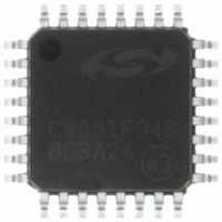
C8051F34B-GQ Silicon Laboratories Inc, C8051F34B-GQ Datasheet - Page 146

C8051F34B-GQ
Manufacturer Part Number
C8051F34B-GQ
Description
IC 8051 MCU 32K FLASH 32LQFP
Manufacturer
Silicon Laboratories Inc
Series
C8051F34xr
Datasheet
1.C8051F349-GQ.pdf
(276 pages)
Specifications of C8051F34B-GQ
Program Memory Type
FLASH
Program Memory Size
32KB (32K x 8)
Package / Case
32-LQFP
Core Processor
8051
Core Size
8-Bit
Speed
48MHz
Connectivity
SMBus (2-Wire/I²C), SPI, UART/USART, USB
Peripherals
Brown-out Detect/Reset, POR, PWM, Temp Sensor, WDT
Number Of I /o
25
Ram Size
2.25K x 8
Voltage - Supply (vcc/vdd)
2.7 V ~ 3.6 V
Data Converters
A/D 17x10b
Oscillator Type
Internal
Operating Temperature
-40°C ~ 85°C
Processor Series
C8051F3x
Core
8051
Data Bus Width
8 bit
Data Ram Size
2.25 KB
Interface Type
I2C/SMBus/SPI/UART/USB
Maximum Clock Frequency
48 MHz
Number Of Programmable I/os
25
Number Of Timers
4
Maximum Operating Temperature
+ 85 C
Mounting Style
SMD/SMT
3rd Party Development Tools
KSK-SL-F34X, KSK-SL-TOOLSTICK, PK51, CA51, A51, ULINK2
Development Tools By Supplier
C8051F340DK
Minimum Operating Temperature
- 40 C
Package
32LQFP
Device Core
8051
Family Name
C8051F34x
Maximum Speed
48 MHz
Operating Supply Voltage
3.3|5 V
On-chip Adc
17-chx10-bit
Lead Free Status / RoHS Status
Lead free / RoHS Compliant
For Use With
336-1748 - ADAPTER TOOLSTICK FOR C8051F34X
Eeprom Size
-
Lead Free Status / Rohs Status
Lead free / RoHS Compliant
Other names
336-1534
Available stocks
Company
Part Number
Manufacturer
Quantity
Price
Company:
Part Number:
C8051F34B-GQ
Manufacturer:
Silicon Laboratories Inc
Quantity:
10 000
Company:
Part Number:
C8051F34B-GQR
Manufacturer:
Silicon Laboratories Inc
Quantity:
10 000
- Current page: 146 of 276
- Download datasheet (2Mb)
C8051F340/1/2/3/4/5/6/7/8/9/A/B/C/D
Registers XBR0, XBR1, and XBR2 are used to assign the digital I/O resources to the physical I/O Port
pins. Note that when the SMBus is selected, the Crossbar assigns both pins associated with the SMBus
(SDA and SCL); when either UART is selected, the Crossbar assigns both pins associated with the UART
(TX and RX). UART0 pin assignments are fixed for bootloading purposes: UART TX0 is always assigned
to P0.4; UART RX0 is always assigned to P0.5. Standard Port I/Os appear contiguously after the prioritized
functions have been assigned.
Important Note: The SPI can be operated in either 3-wire or 4-wire modes, depending on the state of the
NSSMD1-NSSMD0 bits in register SPI0CN. According to the SPI mode, the NSS signal may or may not be
routed to a Port pin.
146
Figure 15.5. Crossbar Priority Decoder in Example Configuration (3 Pins Skipped)
S F Signa ls
(32-pin
P a cka ge )
S F Signa ls
(48-pin
P a cka ge )
P IN I/O
TX 0
RX0
S CK
M ISO
M OSI
NSS*
S DA
S CL
CP0
CP0A
CP1
CP1A
S YSCLK
CEX0
CEX1
CEX2
CEX3
CEX4
ECI
T0
T1
TX 1**
RX1**
S F Signa ls
Port pin assigned to peripheral by the Crossbar
Special Function Signals are not assigned by the Crossbar. W hen these signals are
enabled, the Crossbar must be manually configured to skip their corresponding port pins.
0
0
1
0
2
1
P 0SKIP[0:7]
3
1
P 0
4
0
5
0
6
0
7
0
0
1
*NSS is only pinned out in 4-wire S PI m ode
1
0
2
0
P1S KIP[0:7]
3
0
P1
4
0
Rev. 1.3
5
0
6
0
7
0
0
0
**UA RT1 available only on C8051F340/1/4/5/8/A /B devices
1
0
2
0
P2SKIP[0:7]
3
0
P2
4
0
5
0
6
0
7
0
Example:
0
0
1
0
P3.1-P3.7 una va ila ble on
the 32-pin pa cka ge s
2
0
P3SKIP [0:7]
XBR0 = 0x07
XBR1 = 0x43
P 0SK IP = 0x0C
P 1SK IP = 0x01
3
0
P3
4
0
5
0
6
0
7
0
Related parts for C8051F34B-GQ
Image
Part Number
Description
Manufacturer
Datasheet
Request
R
Part Number:
Description:
SMD/C°/SINGLE-ENDED OUTPUT SILICON OSCILLATOR
Manufacturer:
Silicon Laboratories Inc
Part Number:
Description:
Manufacturer:
Silicon Laboratories Inc
Datasheet:
Part Number:
Description:
N/A N/A/SI4010 AES KEYFOB DEMO WITH LCD RX
Manufacturer:
Silicon Laboratories Inc
Datasheet:
Part Number:
Description:
N/A N/A/SI4010 SIMPLIFIED KEY FOB DEMO WITH LED RX
Manufacturer:
Silicon Laboratories Inc
Datasheet:
Part Number:
Description:
N/A/-40 TO 85 OC/EZLINK MODULE; F930/4432 HIGH BAND (REV E/B1)
Manufacturer:
Silicon Laboratories Inc
Part Number:
Description:
EZLink Module; F930/4432 Low Band (rev e/B1)
Manufacturer:
Silicon Laboratories Inc
Part Number:
Description:
I°/4460 10 DBM RADIO TEST CARD 434 MHZ
Manufacturer:
Silicon Laboratories Inc
Part Number:
Description:
I°/4461 14 DBM RADIO TEST CARD 868 MHZ
Manufacturer:
Silicon Laboratories Inc
Part Number:
Description:
I°/4463 20 DBM RFSWITCH RADIO TEST CARD 460 MHZ
Manufacturer:
Silicon Laboratories Inc
Part Number:
Description:
I°/4463 20 DBM RADIO TEST CARD 868 MHZ
Manufacturer:
Silicon Laboratories Inc
Part Number:
Description:
I°/4463 27 DBM RADIO TEST CARD 868 MHZ
Manufacturer:
Silicon Laboratories Inc
Part Number:
Description:
I°/4463 SKYWORKS 30 DBM RADIO TEST CARD 915 MHZ
Manufacturer:
Silicon Laboratories Inc
Part Number:
Description:
N/A N/A/-40 TO 85 OC/4463 RFMD 30 DBM RADIO TEST CARD 915 MHZ
Manufacturer:
Silicon Laboratories Inc
Part Number:
Description:
I°/4463 20 DBM RADIO TEST CARD 169 MHZ
Manufacturer:
Silicon Laboratories Inc


