M30260F8AGP#U3A Renesas Electronics America, M30260F8AGP#U3A Datasheet - Page 20
M30260F8AGP#U3A
Manufacturer Part Number
M30260F8AGP#U3A
Description
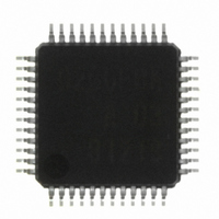
IC M16C/26A MCU FLASH 64K 48LQFP
Manufacturer
Renesas Electronics America
Series
M16C™ M16C/Tiny/26r
Specifications of M30260F8AGP#U3A
Core Processor
M16C/60
Core Size
16-Bit
Speed
20MHz
Connectivity
I²C, IEBus, SIO, UART/USART
Peripherals
DMA, PWM, Voltage Detect, WDT
Number Of I /o
39
Program Memory Size
64KB (64K x 8)
Program Memory Type
FLASH
Ram Size
2K x 8
Voltage - Supply (vcc/vdd)
2.7 V ~ 5.5 V
Data Converters
A/D 12x10b
Oscillator Type
Internal
Operating Temperature
-40°C ~ 85°C
Package / Case
48-LQFP
For Use With
R0K33026AS000BE - KIT DEV EVALUATION M16C/26A
Lead Free Status / RoHS Status
Lead free / RoHS Compliant
Eeprom Size
-
Available stocks
Company
Part Number
Manufacturer
Quantity
Price

Part Number:
M30260F8AGP#U3AM30260F8AGP#D3
Manufacturer:
Renesas Electronics America
Quantity:
10 000
Part Number:
M30260F8AGP#U3AM30260F8AGP#D5
Manufacturer:
Renesas Electronics America
Quantity:
10 000
Part Number:
M30260F8AGP#U3AM30260F8AGP#U3
Manufacturer:
Renesas Electronics America
Quantity:
10 000


M
R
R
e
E
1
. v
2.3 Frame Base Register (FB)
2.4 Interrupt Table Register (INTB)
2.5 Program Counter (PC)
2.6 User Stack Pointer (USP) and Interrupt Stack Pointer (ISP)
2.7 Static Base Register (SB)
2.8 Flag Register (FLG)
J
6
0
FB is configured with 16 bits, and is used for FB relative addressing.
INTB is configured with 20 bits, indicating the start address of an interrupt vector table.
PC is configured with 20 bits, indicating the address of an instruction to be executed.
Stack pointer (SP) comes in two types: USP and ISP, each configured with 16 bits.
Your desired type of stack pointer (USP or ISP) can be selected by the U flag of FLG.
SB is configured with 16 bits, and is used for SB relative addressing.
FLG consists of 11 bits, indicating the CPU status.
2.8.1 Carry Flag (C Flag)
2.8.2 Debug Flag (D Flag)
2.8.3 Zero Flag (Z Flag)
2.8.4 Sign Flag (S Flag)
2.8.5 Register Bank Select Flag (B Flag)
2.8.6 Overflow Flag (O Flag)
2.8.7 Interrupt Enable Flag (I Flag)
2.8.8 Stack Pointer Select Flag (U Flag)
2.8.9 Processor Interrupt Priority Level (IPL)
2.8.10 Reserved Area
C
0
3
This flag retains a carry, borrow, or shift-out bit that has occurred in the arithmetic/logic unit.
The D flag is used exclusively for debugging purpose. During normal use, it must be set to 0.
This flag is set to 1 when an arithmetic operation resulted in 0; otherwise, it is 0.
This flag is set to 1 when an arithmetic operation resulted in a negative value; otherwise, it is 0.
Register bank 0 is selected when this flag is 0 ; register bank 1 is selected when this flag is 1.
This flag is set to 1 when the operation resulted in an overflow; otherwise, it is 0.
This flag enables a maskable interrupt.
Maskable interrupts are disabled when the I flag is 0, and are enabled when the I flag is 1.
The I flag is cleared to 0 when the interrupt request is accepted.
ISP is selected when the U flag is 0; USP is selected when the U flag is 1.
The U flag is cleared to 0 when a hardware interrupt request is accepted or an INT instruction for software
interrupt Nos. 0 to 31 is executed.
IPL is configured with three bits, for specification of up to eight processor interrupt priority levels from level
0 to level 7.
If a requested interrupt has priority greater than IPL, the interrupt is enabled.
When write to this bit, write 0. When read, its content is undefined.
5 .
2 /
B
0
1
6
0
A
7
J
1
l u
G
0 -
2 .
o r
0
, 5
5
u
1
p
2
0
(
0
M
6
1
6
C
page 18
2 /
6
, A
M
f o
1
6
2
C
6
2 /
6
, B
M
1
6
C
2 /
6
) T
2. CPU
Related parts for M30260F8AGP#U3A
Image
Part Number
Description
Manufacturer
Datasheet
Request
R

Part Number:
Description:
KIT STARTER FOR M16C/29
Manufacturer:
Renesas Electronics America
Datasheet:

Part Number:
Description:
KIT STARTER FOR R8C/2D
Manufacturer:
Renesas Electronics America
Datasheet:

Part Number:
Description:
R0K33062P STARTER KIT
Manufacturer:
Renesas Electronics America
Datasheet:

Part Number:
Description:
KIT STARTER FOR R8C/23 E8A
Manufacturer:
Renesas Electronics America
Datasheet:

Part Number:
Description:
KIT STARTER FOR R8C/25
Manufacturer:
Renesas Electronics America
Datasheet:

Part Number:
Description:
KIT STARTER H8S2456 SHARPE DSPLY
Manufacturer:
Renesas Electronics America
Datasheet:

Part Number:
Description:
KIT STARTER FOR R8C38C
Manufacturer:
Renesas Electronics America
Datasheet:

Part Number:
Description:
KIT STARTER FOR R8C35C
Manufacturer:
Renesas Electronics America
Datasheet:

Part Number:
Description:
KIT STARTER FOR R8CL3AC+LCD APPS
Manufacturer:
Renesas Electronics America
Datasheet:
Part Number:
Description:
KIT STARTER FOR RX610
Manufacturer:
Renesas Electronics America
Datasheet:

Part Number:
Description:
KIT STARTER FOR R32C/118
Manufacturer:
Renesas Electronics America
Datasheet:

Part Number:
Description:
KIT DEV RSK-R8C/26-29
Manufacturer:
Renesas Electronics America
Datasheet:

Part Number:
Description:
KIT STARTER FOR SH7124
Manufacturer:
Renesas Electronics America
Datasheet:

Part Number:
Description:
KIT STARTER FOR H8SX/1622
Manufacturer:
Renesas Electronics America
Datasheet:

Part Number:
Description:
KIT DEV FOR SH7203
Manufacturer:
Renesas Electronics America
Datasheet: