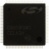
C8051F040-GQ Silicon Laboratories Inc, C8051F040-GQ Datasheet - Page 37

C8051F040-GQ
Manufacturer Part Number
C8051F040-GQ
Description
IC 8051 MCU 64K FLASH 100TQFP
Manufacturer
Silicon Laboratories Inc
Series
C8051F04xr
Datasheets
1.C8051F040-TB.pdf
(328 pages)
2.C8051F040-TB.pdf
(2 pages)
3.C8051F043-GQ.pdf
(328 pages)
Specifications of C8051F040-GQ
Program Memory Type
FLASH
Program Memory Size
64KB (64K x 8)
Package / Case
100-TQFP, 100-VQFP
Core Processor
8051
Core Size
8-Bit
Speed
25MHz
Connectivity
CAN, EBI/EMI, SMBus (2-Wire/I²C), SPI, UART/USART
Peripherals
Brown-out Detect/Reset, POR, PWM, Temp Sensor, WDT
Number Of I /o
64
Ram Size
4.25K x 8
Voltage - Supply (vcc/vdd)
2.7 V ~ 3.6 V
Data Converters
A/D 8x8b, 13x12b; D/A 2x10b, 2x12b
Oscillator Type
Internal
Operating Temperature
-40°C ~ 85°C
Processor Series
C8051F0x
Core
8051
Data Bus Width
8 bit
Data Ram Size
4.25 KB
Interface Type
CAN/SMBus/SPI/UART
Maximum Clock Frequency
25 MHz
Number Of Programmable I/os
64
Number Of Timers
5
Operating Supply Voltage
2.7 V to 3.6 V
Maximum Operating Temperature
+ 85 C
Mounting Style
SMD/SMT
3rd Party Development Tools
PK51, CA51, A51, ULINK2
Development Tools By Supplier
C8051F040DK
Minimum Operating Temperature
- 40 C
On-chip Adc
8-ch x 8-bit or 13-ch x 12-bit
On-chip Dac
2-ch x 12-bit
No. Of I/o's
64
Ram Memory Size
4352Byte
Cpu Speed
25MHz
No. Of Timers
5
Rohs Compliant
Yes
Data Rom Size
64 KB
A/d Bit Size
12 bit
A/d Channels Available
13
Height
1 mm
Length
14 mm
Supply Voltage (max)
3.6 V
Supply Voltage (min)
2.7 V
Width
14 mm
Package
100TQFP
Device Core
8051
Family Name
C8051F04x
Maximum Speed
25 MHz
Lead Free Status / RoHS Status
Lead free / RoHS Compliant
For Use With
336-1205 - DEV KIT FOR F040/F041/F042/F043
Eeprom Size
-
Lead Free Status / Rohs Status
Lead free / RoHS Compliant
Other names
336-1204
Available stocks
Company
Part Number
Manufacturer
Quantity
Price
Company:
Part Number:
C8051F040-GQ
Manufacturer:
SiliconL
Quantity:
702
Company:
Part Number:
C8051F040-GQ
Manufacturer:
Silicon Laboratories Inc
Quantity:
10 000
Company:
Part Number:
C8051F040-GQR
Manufacturer:
Silicon Laboratories Inc
Quantity:
10 000
Part Number:
C8051F040-GQR
Manufacturer:
SILICON LABS/èٹ¯ç§‘
Quantity:
20 000
4.
MONEN
VREFA
VREF0
VREF2
DGND
XTAL1
XTAL2
AIN0.0
AIN0.1
AGND
Name
VREF
VREF
/RST
TMS
TDO
TCK
AV+
V
TDI
DD
Pinout and Package Definitions
F040/2/4/6 F041/3/5/7
37, 64, 90 24, 41, 57
38, 63, 89 25, 40, 56
9, 10, 13
8, 11, 14
Pin Numbers
26
27
28
12
16
17
15
18
19
1
2
3
4
5
3, 6
4, 5
58
59
60
61
62
17
18
19
10
7
8
9
Table 4.1. Pin Definitions
D Out JTAG Test Data Output with internal pullup. Data is shifted out on
A Out Crystal Output. This pin is the excitation driver for a crystal or
D I/O Device Reset. Open-drain output of internal V
Type Description
A I/O Bandgap Voltage Reference Output (all devices).
D In JTAG Test Mode Select with internal pullup.
D In JTAG Test Clock with internal pullup.
D In JTAG Test Data Input with internal pullup. TDI is latched on the
D In V
A In Crystal Input. This pin is the return for the internal oscillator circuit
A In ADC0 (C8051F041/3/5/7) and ADC2 (C8051F041/3 only)
A In ADC0 Voltage Reference Input.
A In ADC2 Voltage Reference Input (C8051F040/2 only).
A In DAC Voltage Reference Input (C8051F040/2 only).
A In ADC0 Input Channel 0 (See ADC0 Specification for complete
A In ADC0 Input Channel 1 (See ADC0 Specification for complete
Digital Supply Voltage. Must be tied to +2.7 to +3.6 V.
Digital Ground. Must be tied to Ground.
Analog Supply Voltage. Must be tied to +2.7 to +3.6 V.
Analog Ground. Must be tied to Ground.
rising edge of TCK.
TDO on the falling edge of TCK. TDO output is a tri-state driver.
driven low when V
source can initiate a system reset by driving this pin low.
for a crystal or ceramic resonator. For a precision internal clock,
connect a crystal or ceramic resonator from XTAL1 to XTAL2. If
overdriven by an external CMOS clock, this becomes the system
clock.
ceramic resonator.
V
When tied low, the internal V
In most applications, MONEN should be connected directly
to V
DAC Voltage Reference Input (C8051F041/3 only).
Voltage Reference Input.
description).
description).
DD
DD
DD
Monitor Enable. When tied high, this pin enables the internal
Rev. 1.4
monitor, which forces a system reset when V
.
C8051F040/1/2/3/4/5/6/7
DD
is < 2.7 V and MONEN is high. An external
DD
monitor is disabled.
DD
monitor. Is
DD
is < 2.7 V.
37


