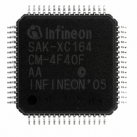
SAK-XC164CM-4F40F AA Infineon Technologies, SAK-XC164CM-4F40F AA Datasheet - Page 41

SAK-XC164CM-4F40F AA
Manufacturer Part Number
SAK-XC164CM-4F40F AA
Description
IC MCU 16BIT 32KB FLSH TQFP-64-8
Manufacturer
Infineon Technologies
Series
XC16xr
Datasheet
1.SAF-XC164CM-4F20F_AA.pdf
(70 pages)
Specifications of SAK-XC164CM-4F40F AA
Core Processor
C166SV2
Core Size
16-Bit
Speed
40MHz
Connectivity
CAN, SPI, UART/USART
Peripherals
PWM, WDT
Number Of I /o
47
Program Memory Size
32KB (32K x 8)
Program Memory Type
FLASH
Ram Size
4K x 8
Voltage - Supply (vcc/vdd)
2.35 V ~ 2.7 V
Data Converters
A/D 14x8/10b
Oscillator Type
Internal
Operating Temperature
-40°C ~ 125°C
Package / Case
64-LFQFP
For Use With
B158-H8961-X-X-7600IN - KIT EASY XC164CMXC164CMUCANIN - KIT U-CAN STARTER XC164CMMCBX167-NET - BOARD EVAL INFINEON CAN/ETHRNTMCBXC167-BASIC - BOARD EVAL BASIC INFINEON XC16X
Lead Free Status / RoHS Status
Lead free / RoHS Compliant
Eeprom Size
-
Other names
SAK-XC164CM-4F40FAACT
SAK-XC164CM-4F40FAACT
SAK-XC164CM-4F40FAAINCT
SAK-XC164CM-4F40FAACT
SAK-XC164CM-4F40FAAINCT
3.12
The integrated TwinCAN module handles the completely autonomous transmission and
reception of CAN frames in accordance with the CAN specification V2.0 part B (active),
i.e. the on-chip TwinCAN module can receive and transmit standard frames with 11-bit
identifiers as well as extended frames with 29-bit identifiers.
Two Full-CAN nodes share the TwinCAN module’s resources to optimize the CAN bus
traffic handling and to minimize the CPU load. The module provides up to 32 message
objects, which can be assigned to one of the CAN nodes and can be combined to FIFO-
structures. Each object provides separate masks for acceptance filtering.
The flexible combination of Full-CAN functionality and FIFO architecture reduces the
efforts to fulfill the real-time requirements of complex embedded control applications.
Improved CAN bus monitoring functionality as well as the number of message objects
permit precise and comfortable CAN bus traffic handling.
Gateway functionality allows automatic data exchange between two separate CAN bus
systems, which reduces CPU load and improves the real time behavior of the entire
system.
The bit timing for both CAN nodes is derived from the master clock and is programmable
up to a data rate of 1 Mbit/s. Each CAN node uses two pins of Port 9 to interface to an
external bus transceiver. The interface pins are assigned via software.
Figure 10
Data Sheet
Decoder
Address
Interrupt
Control
Control
Clock
TwinCAN Module
TwinCAN Module Block Diagram
f
CAN
TwinCAN Module Kernel
Node A
TwinCAN Control
CAN
Message
Object
Buffer
Node B
CAN
39
RxDCA
RxDCB
TxDCA
TxDCB
Functional Description
Control
Port
Derivatives
V1.4, 2007-03
MCB05567
XC164CM


