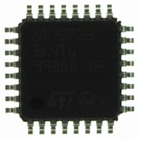
ST72F325K4T6 STMicroelectronics, ST72F325K4T6 Datasheet - Page 116

ST72F325K4T6
Manufacturer Part Number
ST72F325K4T6
Description
MCU 8BIT 16KB FLASH/ROM 32-LQFP
Manufacturer
STMicroelectronics
Series
ST7r
Datasheet
1.ST72F325K6T6.pdf
(197 pages)
Specifications of ST72F325K4T6
Core Processor
ST7
Core Size
8-Bit
Speed
8MHz
Connectivity
I²C, SCI, SPI
Peripherals
LVD, POR, PWM, WDT
Number Of I /o
24
Program Memory Size
16KB (16K x 8)
Program Memory Type
FLASH
Ram Size
512 x 8
Voltage - Supply (vcc/vdd)
3.8 V ~ 5.5 V
Data Converters
A/D 16x10b
Oscillator Type
Internal
Operating Temperature
-40°C ~ 85°C
Package / Case
32-LQFP
Processor Series
ST72F3x
Core
ST7
Data Bus Width
8 bit
Data Ram Size
512 B
Interface Type
I2C, SCI, SPI
Maximum Clock Frequency
8 MHz
Number Of Programmable I/os
48
Number Of Timers
2
Maximum Operating Temperature
+ 85 C
Mounting Style
SMD/SMT
Development Tools By Supplier
ST7232X-EVAL, ST7232X-SK/RAIS, ST72325-D/RAIS, ST7MDT20-DVP3, ST7MDT20J-EMU3, ST7MDT20M-EMU3, STX-RLINK
Minimum Operating Temperature
- 40 C
On-chip Adc
10 bit, 16 Channel
For Use With
497-5046 - KIT TOOL FOR ST7/UPSD/STR7 MCU
Lead Free Status / RoHS Status
Lead free / RoHS Compliant
Eeprom Size
-
Lead Free Status / Rohs Status
Details
Other names
497-5605
Available stocks
Company
Part Number
Manufacturer
Quantity
Price
Company:
Part Number:
ST72F325K4T6
Manufacturer:
ST
Quantity:
151
Company:
Part Number:
ST72F325K4T6
Manufacturer:
STMicroelectronics
Quantity:
10 000
Part Number:
ST72F325K4T6
Manufacturer:
ST
Quantity:
20 000
Company:
Part Number:
ST72F325K4T6TR
Manufacturer:
STMicroelectronics
Quantity:
10 000
ST72325xx
SERIAL COMMUNICATIONS INTERFACE (Cont’d)
DATA REGISTER (SCIDR)
Read/Write
Reset Value: Undefined
Contains the Received or Transmitted data char-
acter, depending on whether it is read from or writ-
ten to.
The Data register performs a double function (read
and write) since it is composed of two registers,
one for transmission (TDR) and one for reception
(RDR).
The TDR register provides the parallel interface
between the internal bus and the output shift reg-
ister (see
The RDR register provides the parallel interface
between the input shift register and the internal
bus (see
BAUD RATE REGISTER (SCIBRR)
Read/Write
Reset Value: 0000 0000 (00h)
Bits 7:6 = SCP[1:0] First SCI Prescaler
These 2 prescaling bits allow several standard
clock division ranges:
116/197
SCP1
DR7
7
7
PR Prescaling factor
SCP0
DR6
Figure
Figure
13
SCT2
1
3
4
DR5
1.).
1.).
SCT1
DR4
SCT0
DR3
SCP1
SCR2 SCR1 SCR0
DR2
0
0
1
1
DR1
SCP0
0
1
0
1
DR0
0
0
Bits 5:3 = SCT[2:0] SCI Transmitter rate divisor
These 3 bits, in conjunction with the SCP1 & SCP0
bits define the total division applied to the bus
clock to yield the transmit rate clock in convention-
al Baud Rate Generator mode.
Bits 2:0 = SCR[2:0] SCI Receiver rate divisor.
These 3 bits, in conjunction with the SCP[1:0] bits
define the total division applied to the bus clock to
yield the receive rate clock in conventional Baud
Rate Generator mode.
RR Dividing factor
TR dividing factor
128
128
16
32
64
16
32
64
1
2
4
8
1
2
4
8
SCR2
SCT2
0
0
0
0
1
1
1
1
0
0
0
0
1
1
1
1
SCR1
SCT1
0
0
1
1
0
0
1
1
0
0
1
1
0
0
1
1
SCR0
SCT0
0
1
0
1
0
1
0
1
0
1
0
1
0
1
0
1


