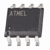
ATTINY13-20SU Atmel, ATTINY13-20SU Datasheet - Page 16

ATTINY13-20SU
Manufacturer Part Number
ATTINY13-20SU
Description
IC MCU AVR 1K FLASH 20MHZ 8SOIC
Manufacturer
Atmel
Series
AVR® ATtinyr
Specifications of ATTINY13-20SU
Core Processor
AVR
Core Size
8-Bit
Speed
20MHz
Peripherals
Brown-out Detect/Reset, POR, PWM, WDT
Number Of I /o
6
Program Memory Size
1KB (512 x 16)
Program Memory Type
FLASH
Eeprom Size
64 x 8
Ram Size
64 x 8
Voltage - Supply (vcc/vdd)
2.7 V ~ 5.5 V
Data Converters
A/D 4x10b
Oscillator Type
Internal
Operating Temperature
-40°C ~ 85°C
Package / Case
8-SOIC (5.3mm Width), 8-SOP, 8-SOEIAJ
Package
8SOIC EIAJ
Device Core
AVR
Family Name
ATtiny
Maximum Speed
20 MHz
Operating Supply Voltage
3.3|5 V
Data Bus Width
8 Bit
Number Of Programmable I/os
6
Interface Type
SPI
On-chip Adc
4-chx10-bit
Number Of Timers
1
For Use With
ATSTK600-DIP40 - STK600 SOCKET/ADAPTER 40-PDIP770-1007 - ISP 4PORT ATMEL AVR MCU SPI/JTAG770-1004 - ISP 4PORT FOR ATMEL AVR MCU SPIATAVRDRAGON - KIT DRAGON 32KB FLASH MEM AVRATAVRISP2 - PROGRAMMER AVR IN SYSTEMATJTAGICE2 - AVR ON-CHIP D-BUG SYSTEM
Lead Free Status / RoHS Status
Lead free / RoHS Compliant
Connectivity
-
- Current page: 16 of 176
- Download datasheet (3Mb)
5.2.1
5.3
5.3.1
16
EEPROM Data Memory
ATtiny13
Data Memory Access Times
EEPROM Read/Write Access
The 32 general purpose working registers, 64 I/O Registers, and the 64 bytes of internal data
SRAM in the ATtiny13 are all accessible through all these addressing modes. The Register File
is described in
Figure 5-2.
This section describes the general access timing concepts for internal memory access. The
internal data SRAM access is performed in two clk
Figure 5-3.
The ATtiny13 contains 64 bytes of data EEPROM memory. It is organized as a separate data
space, in which single bytes can be read and written. The EEPROM has an endurance of at
least 100,000 write/erase cycles. The access between the EEPROM and the CPU is described
in the following, specifying the EEPROM Address Registers, the EEPROM Data Register, and
the EEPROM Control Register. For a detailed description of Serial data downloading to the
EEPROM, see
The EEPROM Access Registers are accessible in the I/O space.
Data Memory Map
On-chip Data SRAM Access Cycles
“General Purpose Register File” on page
page
Address
clk
Data
Data
WR
CPU
RD
105.
Compute Address
64 I/O Registers
Data Memory
Internal SRAM
32 Registers
T1
(64 x 8)
Memory Access Instruction
Address valid
0x009F
0x0000 - 0x001F
0x0020 - 0x005F
0x0060
CPU
T2
cycles as described in
10.
Next Instruction
T3
Figure
2535J–AVR–08/10
5-3.
Related parts for ATTINY13-20SU
Image
Part Number
Description
Manufacturer
Datasheet
Request
R

Part Number:
Description:
IC MCU AVR 1K FLASH 20MHZ 8SOIC
Manufacturer:
Atmel
Datasheet:

Part Number:
Description:
Manufacturer:
Atmel Corporation
Datasheet:

Part Number:
Description:
IC MCU AVR 1K FLASH 20MHZ 8SOIC
Manufacturer:
Atmel
Datasheet:

Part Number:
Description:
IC MCU AVR 1K FLASH 10MHZ 20-MLF
Manufacturer:
Atmel
Datasheet:

Part Number:
Description:
IC MCU AVR 1K FLASH 20MHZ 8DIP
Manufacturer:
Atmel
Datasheet:

Part Number:
Description:
MCU AVR 1KB FLASH 20MHZ 3X3 QFN
Manufacturer:
Atmel
Datasheet:

Part Number:
Description:
IC MCU AVR 1K 5V 20MHZ 8DIP
Manufacturer:
Atmel
Datasheet:

Part Number:
Description:
IC MCU AVR 1K 5V 20MHZ 8SOIC
Manufacturer:
Atmel
Datasheet:

Part Number:
Description:
IC MCU AVR 1K 5V 20MHZ 8SOIC
Manufacturer:
Atmel
Datasheet:

Part Number:
Description:
IC MCU AVR 1K FLASH 20MHZ 8DIP
Manufacturer:
Atmel
Datasheet:

Part Number:
Description:
IC MCU AVR 1K FLASH 20MHZ 8SOIC
Manufacturer:
Atmel
Datasheet:

Part Number:
Description:
MCU AVR 1KB FLASH 20MHZ 8SOIC GW
Manufacturer:
Atmel
Datasheet:


