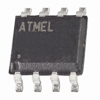
ATTINY25V-15ST Atmel, ATTINY25V-15ST Datasheet - Page 133

ATTINY25V-15ST
Manufacturer Part Number
ATTINY25V-15ST
Description
MCU AVR 2K FLASH 4MHZ 8-SOIC
Manufacturer
Atmel
Series
AVR® ATtinyr
Datasheet
1.ATTINY25-15MZ.pdf
(196 pages)
Specifications of ATTINY25V-15ST
Package / Case
8-SOIC (3.9mm Width)
Voltage - Supply (vcc/vdd)
1.8 V ~ 3.6 V
Operating Temperature
-40°C ~ 85°C
Speed
8MHz
Number Of I /o
6
Eeprom Size
128 x 8
Core Processor
AVR
Program Memory Type
FLASH
Ram Size
128 x 8
Program Memory Size
2KB (2K x 8)
Data Converters
A/D 4x10b
Oscillator Type
Internal
Peripherals
Brown-out Detect/Reset, POR, PWM, WDT
Connectivity
USI
Core Size
8-Bit
Processor Series
ATTINY2x
Core
AVR8
Data Bus Width
8 bit
Data Ram Size
128 B
Maximum Operating Temperature
+ 85 C
Mounting Style
SMD/SMT
Lead Free Status / RoHS Status
Lead free / RoHS Compliant
Available stocks
Company
Part Number
Manufacturer
Quantity
Price
Part Number:
ATTINY25V-15ST
Manufacturer:
ATMEL/爱特梅尔
Quantity:
20 000
- Current page: 133 of 196
- Download datasheet (4Mb)
20.4.2
20.4.3
20.4.4
7598H–AVR–07/09
EEPROM Write Prevents Writing to SPMCSR
Reading the Fuse and Lock Bits from Software
Preventing Flash Corruption
Note that an EEPROM write operation will block all software programming to Flash. Reading the
Fuses and Lock bits from software will also be prevented during the EEPROM write operation. It
is recommended that the user checks the status bit (EEWE) in the EECR Register and verifies
that the bit is cleared before writing to the SPMCSR Register.
It is possible to read both the Fuse and Lock bits from software. To read the Lock bits, load the
Z-pointer with 0x0001 and set the RFLB and SPMEN bits in SPMCSR. When an LPM instruction
is executed within three CPU cycles after the RFLB and SPMEN bits are set in SPMCSR, the
value of the Lock bits will be loaded in the destination register. The RFLB and SPMEN bits will
auto-clear upon completion of reading the Lock bits or if no LPM instruction is executed within
three CPU cycles or no SPM instruction is executed within four CPU cycles. When RFLB and
SPMEN are cleared, LPM will work as described in the Instruction set Manual.
The algorithm for reading the Fuse Low byte is similar to the one described above for reading
the Lock bits. To read the Fuse Low byte, load the Z-pointer with 0x0000 and set the RFLB and
SPMEN bits in SPMCSR. When an LPM instruction is executed within three cycles after the
RFLB and SPMEN bits are set in the SPMCSR, the value of the Fuse Low byte (FLB) will be
loaded in the destination register as shown below. Refer to
detailed description and mapping of the Fuse Low byte.
Similarly, when reading the Fuse High byte, load 0x0003 in the Z-pointer. When an LPM instruc-
tion is executed within three cycles after the RFLB and SPMEN bits are set in the SPMCSR, the
value of the Fuse High byte (FHB) will be loaded in the destination register as shown below.
Refer to
Fuse and Lock bits that are programmed, will be read as zero. Fuse and Lock bits that are
unprogrammed, will be read as one.
During periods of low V
too low for the CPU and the Flash to operate properly. These issues are the same as for board
level systems using the Flash, and the same design solutions should be applied.
A Flash program corruption can be caused by two situations when the voltage is too low. First, a
regular write sequence to the Flash requires a minimum voltage to operate correctly. Secondly,
the CPU itself can execute instructions incorrectly, if the supply voltage for executing instructions
is too low.
Bit
Rd
Bit
Rd
Bit
Rd
Table 21-4
FHB7
FLB7
7
7
7
–
for detailed description and mapping of the Fuse High byte.
CC
FLB6
FHB6
, the Flash program can be corrupted because the supply voltage is
6
–
6
6
FHB5
FLB5
5
5
5
–
FHB4
FLB4
4
–
4
4
FLB3
FHB3
3
–
3
3
FHB2
FLB2
2
–
2
2
Table 21-5 on page 136
ATtiny25/45/85
FHB1
FLB1
LB2
1
1
1
FLB0
FHB0
LB1
0
0
0
for a
133
Related parts for ATTINY25V-15ST
Image
Part Number
Description
Manufacturer
Datasheet
Request
R

Part Number:
Description:
IC MCU AVR 2K FLASH 10MHZ 20-QFN
Manufacturer:
Atmel
Datasheet:

Part Number:
Description:
MCU AVR 2KB FLASH 10MHZ 8SOIC
Manufacturer:
Atmel
Datasheet:

Part Number:
Description:
IC AVR MCU 2K 10MHZ 8-DIP
Manufacturer:
Atmel
Datasheet:

Part Number:
Description:
IC MCU AVR 2KB FLASH 10MHZ 8SOIC
Manufacturer:
Atmel
Datasheet:

Part Number:
Description:
IC MCU AVR 2KB FLASH 10MHZ 8SOIC
Manufacturer:
Atmel
Datasheet:

Part Number:
Description:
MCU AVR 2KB FLASH 10MHZ 8SOIC
Manufacturer:
Atmel
Datasheet:

Part Number:
Description:
MCU AVR 2KB FLASH 10MHZ 20QFN
Manufacturer:
Atmel
Datasheet:

Part Number:
Description:
MCU AVR 2K ISP FLASH 1.8V 8-SOIC
Manufacturer:
Atmel
Datasheet:

Part Number:
Description:
IC AVR MCU 2K 10MHZ 8DIP
Manufacturer:
Atmel
Datasheet:

Part Number:
Description:
IC AVR MCU 2K 10MHZ 8SOIC
Manufacturer:
Atmel
Datasheet:

Part Number:
Description:
8-bit Microcontrollers - MCU 2KB FLASH,128B EE, 128B SRAM-10MHz
Manufacturer:
Atmel

Part Number:
Description:
8-bit Microcontrollers - MCU 2KB FL,128B EE,128B SRAM-10MHz
Manufacturer:
Atmel

Part Number:
Description:
8-bit Microcontrollers - MCU AVR 16KB FL 512B EE 1KB SRAM 10 MHZ GRN
Manufacturer:
Atmel


