PIC24FJ128GA106-E/MR Microchip Technology, PIC24FJ128GA106-E/MR Datasheet - Page 4
PIC24FJ128GA106-E/MR
Manufacturer Part Number
PIC24FJ128GA106-E/MR
Description
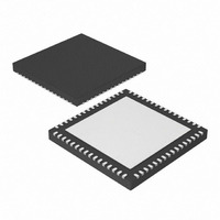
IC PIC MCU FLASH 128K 64-QFN
Manufacturer
Microchip Technology
Series
PIC® 24Fr
Datasheets
1.PIC24FJ128GA106-IPT.pdf
(14 pages)
2.PIC24FJ128GA106-IPT.pdf
(330 pages)
3.PIC24FJ128GA106-IPT.pdf
(52 pages)
4.PIC24FJ128GA110-EPT.pdf
(310 pages)
Specifications of PIC24FJ128GA106-E/MR
Program Memory Type
FLASH
Program Memory Size
128KB (43K x 24)
Package / Case
64-VFQFN, Exposed Pad
Core Processor
PIC
Core Size
16-Bit
Speed
32MHz
Connectivity
I²C, PMP, SPI, UART/USART
Peripherals
Brown-out Detect/Reset, POR, PWM, WDT
Number Of I /o
53
Ram Size
16K x 8
Voltage - Supply (vcc/vdd)
2 V ~ 3.6 V
Data Converters
A/D 16x10b
Oscillator Type
Internal
Operating Temperature
-40°C ~ 125°C
Processor Series
PIC24FJ
Core
PIC
Data Bus Width
16 bit
Data Ram Size
16 KB
Interface Type
I2C/SPI/UART
Maximum Clock Frequency
32 MHz
Number Of Programmable I/os
53
Number Of Timers
5
Maximum Operating Temperature
+ 125 C
Mounting Style
SMD/SMT
3rd Party Development Tools
52713-733, 52714-737, 53276-922, EWDSPIC
Development Tools By Supplier
PG164130, DV164035, DV244005, DV164005, PG164120, DM240001
Minimum Operating Temperature
- 40 C
On-chip Adc
16-ch x 10-bit
Lead Free Status / RoHS Status
Lead free / RoHS Compliant
Eeprom Size
-
Lead Free Status / Rohs Status
Lead free / RoHS Compliant


PIC24FJ256GA110 FAMILY
6. Module: SPI (Master Mode)
EXAMPLE 1:
DS80368J-page 4
In Master mode, both the SPI Interrupt Flag
(SPIxIF) and the SPIRBF bit (SPIxSTAT<0>) may
become set one-half clock cycle early, instead of
on the clock edge. This occurs only under the
following circumstances:
• Enhanced Buffer mode is disabled
• the module is configured for serial data output
If the application is using the interrupt flag to deter-
mine when data to be transmitted is written to the
transmit buffer, the data currently in the buffer may
be overwritten.
Work around
Before writing to the SPI buffer, check the SCK pin
to determine if the last clock edge has passed.
Example 1
doing this. In this example, pin RD1 functions as the
SPI clock, SCK, which is configured as Idle low.
Affected Silicon Revisions
while(IFS0bits.SPI1IF == 0){}
while(PORTDbits.RD1 == 1){}
SPI1BUF = 0xFF;
A3
(SPIBEN = 0); and
changes on transition from clock active to clock
Idle state (CKE = 1)
X
A5
(below) demonstrates a method for
CHECKING THE STATE OF SPIxIF AGAINST THE SPI CLOCK
//wait for the transmission to complete
//wait for the last clock to finish
//write new data to the buffer
7. Module: CTMU
When the CTMU module is selected as the trigger
source (SYNCSEL<4:0> = 11000), the input
capture and/or output compare trigger may not
work.
Work around
Manually trigger the input capture and/or output
compare module(s) after a CTMU event is
received. Be certain to compensate for any time
latency that results from manually triggering the
module.
Affected Silicon Revisions
A3
X
A5
2010 Microchip Technology Inc.
Related parts for PIC24FJ128GA106-E/MR
Image
Part Number
Description
Manufacturer
Datasheet
Request
R

Part Number:
Description:
General Purpose, 16-Bit Flash Microcontrollers
Manufacturer:
MICROCHIP [Microchip Technology]
Datasheet:

Part Number:
Description:
Manufacturer:
Microchip Technology Inc.
Datasheet:
Part Number:
Description:
Manufacturer:
Microchip Technology Inc.
Datasheet:
Part Number:
Description:
Manufacturer:
Microchip Technology Inc.
Datasheet:
Part Number:
Description:
Manufacturer:
Microchip Technology Inc.
Datasheet:
Part Number:
Description:
Manufacturer:
Microchip Technology Inc.
Datasheet:
Part Number:
Description:
Manufacturer:
Microchip Technology Inc.
Datasheet:
Part Number:
Description:
Manufacturer:
Microchip Technology Inc.
Datasheet:
Part Number:
Description:
Manufacturer:
Microchip Technology Inc.
Datasheet: