PIC12C509A/JW Microchip Technology, PIC12C509A/JW Datasheet - Page 67
PIC12C509A/JW
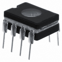
Manufacturer Part Number
PIC12C509A/JW
Description
IC MCU EPROM 1KX12 8CDIP
Manufacturer
Microchip Technology
Series
PIC® 12Cr
Datasheets
1.PIC12C508A-04SM.pdf
(113 pages)
2.PIC12C508A-04SM.pdf
(6 pages)
3.PIC12C508A-04SM.pdf
(16 pages)
4.PIC12C508A-04SM.pdf
(4 pages)
Specifications of PIC12C509A/JW
Core Processor
PIC
Core Size
8-Bit
Speed
4MHz
Peripherals
POR, WDT
Number Of I /o
5
Program Memory Size
1.5KB (1K x 12)
Program Memory Type
EPROM, UV
Ram Size
41 x 8
Voltage - Supply (vcc/vdd)
3 V ~ 5.5 V
Oscillator Type
Internal
Operating Temperature
0°C ~ 70°C
Package / Case
8-CDIP (0.300", 7.62mm) Window
For Use With
DVMCPA - KIT DVR BOARD EVAL SYSTEM MXDEV1DVA12XP080 - ADAPTER DEVICE FOR MPLAB-ICE
Lead Free Status / RoHS Status
Lead free / RoHS Compliant
Eeprom Size
-
Data Converters
-
Connectivity
-
Other names
PIC12C509A/JWR
PIC12C509A/JWR
PIC12C509A/JWR
Available stocks
Company
Part Number
Manufacturer
Quantity
Price
Company:

Part Number:
PIC12C509A/JW
Manufacturer:
Microchip Technology
Quantity:
135
Company:
Part Number:
PIC12C509A/JW
Manufacturer:
MICROCHIP
Quantity:
99


11.2
DC CHARACTERISTICS
D030
D031
D032
D033
D033
D040
D040A
D041
D042
D042A OSC1 (XT and LP)
D043
D070
D060
D061
D063
D080
D090
D100
D101
Note 1: In EXTRC oscillator configuration, the OSC1/CLKIN pin is a Schmitt Trigger input. It is not recommended that
Param
1999 Microchip Technology Inc.
No.
†
2: The leakage current on the MCLR pin is strongly dependent on the applied voltage level. The specified levels
3: Negative current is defined as coming out of the pin.
Input Low Voltage
I/O ports
MCLR, GP2/T0CKI (in EXTRC mode)
OSC1 (EXTRC)
OSC1 (in XT and LP)
Input High Voltage
I/O ports
MCLR/GP2/T0CKI
OSC1 (in EXTRC mode)
GPIO weak pull-up current
Input Leakage Current
I/O ports
MCLR, GP2/T0CKI
OSC1
Output Low Voltage
I/O ports/CLKOUT
Output High Voltage
I/O ports/CLKOUT
Capacitive Loading Specs on
Output Pins
OSC2 pin
All I/O pins
DC CHARACTERISTICS:
Data in “Typ” column is at 5V, 25 C unless otherwise stated. These parameters are for design guidance only
and are not tested.
the PIC12C5XX be driven with external clock in RC mode.
represent normal operating conditions. Higher leakage current may be measured at different input voltages.
with TTL buffer
with Schmitt Trigger buffer
with TTL buffer
with Schmitt Trigger buffer
Characteristic
(1)
(3)
(2, 3)
PIC12C508/509 (Commercial, Industrial, Extended)
Standard Operating Conditions (unless otherwise specified)
Operating temperature
Operating voltage V
Section 11.2.
C
Sym
I
V
V
V
V
C
V
PUR
OSC2
I
OL
OH
SS
IL
IH
IO
IL
0.25V
V
0.85V
0.85V
0.85V
0.7V
DD
2.0V
0.8V
Min
V
V
V
V
V
50
20
-1
-3
SS
SS
SS
SS
SS
-
-
-
- 0.7
DD
DD
DD
DD
DD
+
Typ†
DD
250
130
0.5
0.5
0.5
-
-
-
-
-
-
-
-
-
-
-
-
-
-
-
-
-
-
range as described in DC spec Section 11.1 and
0.15V
0.15V
0.15V
0.15V
–40°C
–40°C
0.3V
Max
0.8V
V
V
V
V
V
V
400
250
0°C
0.6
+1
+5
+3
15
50
DD
DD
DD
DD
DD
DD
-
DD
DD
DD
DD
DD
T
T
T
Units
A
A
A
pF In XT and LP modes when
pF
V
V
V
V
V
V
V
V
V
V
V
V
V
A V
A Vss
A
A
A Vss
+85°C (industrial)
+125°C (extended)
+70°C (commercial)
PIC12C5XX
4.5
otherwise
Note1
4.5
otherwise
For entire V
Note1
For V
Pin at hi-impedance
V
V
XT and LP options
I
I
external clock is used to drive
OSC1.
OL
OH
DD
PIN
PIN
= 8.7 mA, V
= -5.4 mA, V
= 5V, V
= V
= V
DD
V
V
V
V
DD
DD
PIN
PIN
SS
DD
Conditions
5.5V
+ 0.25V
DS40139E-page 67
DD
PIN
5.5V
5.5V
V
V
DD
DD
range
= V
DD
DD
,
,
= 4.5V
SS
(2)
= 4.5V
Related parts for PIC12C509A/JW
Image
Part Number
Description
Manufacturer
Datasheet
Request
R

Part Number:
Description:
8-Pin/ 8-Bit CMOS Microcontrollers
Manufacturer:
Microchip Technology
Part Number:
Description:
8-Pin/ 8-Bit CMOS Microcontroller with EEPROM Data Memory
Manufacturer:
Microchip Technology
Part Number:
Description:
IC, 8BIT MCU, PIC12, 32MHZ, DFN-8
Manufacturer:
Microchip Technology
Datasheet:
Part Number:
Description:
IC, 8BIT MCU, PIC12, 32MHZ, DFN-8
Manufacturer:
Microchip Technology
Datasheet:

Part Number:
Description:
Manufacturer:
Microchip Technology Inc.
Datasheet:
Part Number:
Description:
Manufacturer:
Microchip Technology Inc.
Datasheet:
Part Number:
Description:
Manufacturer:
Microchip Technology Inc.
Datasheet:
Part Number:
Description:
Manufacturer:
Microchip Technology Inc.
Datasheet:
Part Number:
Description:
Manufacturer:
Microchip Technology Inc.
Datasheet:
Part Number:
Description:
Manufacturer:
Microchip Technology Inc.
Datasheet:
Part Number:
Description:
Manufacturer:
Microchip Technology Inc.
Datasheet: