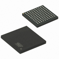
AT91SAM7X512-CU Atmel, AT91SAM7X512-CU Datasheet - Page 283

AT91SAM7X512-CU
Manufacturer Part Number
AT91SAM7X512-CU
Description
MCU ARM 512K HS FLASH 100-TFBGA
Manufacturer
Atmel
Series
AT91SAMr
Datasheet
1.AT91SAM7X512-AU-999.pdf
(687 pages)
Specifications of AT91SAM7X512-CU
Core Processor
ARM7
Core Size
16/32-Bit
Speed
55MHz
Connectivity
CAN, Ethernet, I²C, SPI, SSC, UART/USART, USB
Peripherals
Brown-out Detect/Reset, DMA, POR, PWM, WDT
Number Of I /o
62
Program Memory Size
512KB (512K x 8)
Program Memory Type
FLASH
Ram Size
128K x 8
Voltage - Supply (vcc/vdd)
1.65 V ~ 1.95 V
Data Converters
A/D 8x10b
Oscillator Type
Internal
Operating Temperature
-40°C ~ 85°C
Package / Case
100-TFBGA
Processor Series
AT91SAMx
Core
ARM7TDMI
Data Bus Width
32 bit
Data Ram Size
128 KB
Interface Type
CAN, SPI, SSC, TWI, USART, USB
Maximum Clock Frequency
55 MHz
Number Of Programmable I/os
13
Number Of Timers
3
Operating Supply Voltage
3 V to 3.6 V
Maximum Operating Temperature
+ 85 C
Mounting Style
SMD/SMT
3rd Party Development Tools
JTRACE-ARM-2M, KSK-AT91SAM7X-PL, MDK-ARM, RL-ARM, ULINK2
Development Tools By Supplier
AT91SAM-ICE, AT91-ISP, AT91SAM7X-EK
Minimum Operating Temperature
- 40 C
On-chip Adc
10 bit
Package
100TFBGA
Device Core
ARM7TDMI
Family Name
91S
Maximum Speed
55 MHz
Cpu Family
91S
Device Core Size
32b
Frequency (max)
55MHz
Total Internal Ram Size
128KB
# I/os (max)
62
Number Of Timers - General Purpose
3
Operating Supply Voltage (typ)
1.8/3.3V
Operating Supply Voltage (max)
1.95/3.6V
Operating Supply Voltage (min)
1.65/3V
Instruction Set Architecture
RISC
Operating Temp Range
-40C to 85C
Operating Temperature Classification
Industrial
Mounting
Surface Mount
Pin Count
100
Package Type
TFBGA
For Use With
AT91SAM-ICE - EMULATOR FOR AT91 ARM7/ARM9AT91SAM7X-EK - KIT EVAL FOR AT91SAM7X256/128
Lead Free Status / RoHS Status
Lead free / RoHS Compliant
Eeprom Size
-
Lead Free Status / Rohs Status
Lead free / RoHS Compliant
Available stocks
Company
Part Number
Manufacturer
Quantity
Price
- Current page: 283 of 687
- Download datasheet (11Mb)
29.5
29.5.1
29.5.2
29.5.3
6120H–ATARM–17-Feb-09
Functional Description
Transfer format
Modes of Operation
Master Transmitter Mode
The data put on the TWD line must be 8 bits long. Data is transferred MSB first; each byte must
be followed by an acknowledgement. The number of bytes per transfer is unlimited (see
29-4 on page
Each transfer begins with a START condition and terminates with a STOP condition (see
29-3 on page
Figure 29-3.
Figure 29-4. Transfer Format
The TWI has two modes of operation:
The TWI Control Register (TWI_CR) allows configuration of the interface in Master Mode. In this
mode, it generates the clock according to the value programmed in the Clock Waveform Gener-
ator Register (TWI_CWGR). This register defines the TWCK signal completely, enabling the
interface to be adapted to a wide range of clocks.
After the master initiates a Start condition when writing into the Transmit Holding Register,
TWI_THR, it sends a 7-bit slave address, configured in the Master Mode register (DADR in
TWI_MMR), to notify the slave device. The bit following the slave address indicates the transfer
direction, 0 in this case (MREAD = 0 in TWI_MMR).
The TWI transfers require the slave to acknowledge each received byte. During the acknowl-
edge clock pulse (9th pulse), the master releases the data line (HIGH), enabling the slave to pull
it down in order to generate the acknowledge. The master polls the data line during this clock
pulse and sets the Not Acknowledge bit (NACK) in the status register if the slave does not
• A high-to-low transition on the TWD line while TWCK is high defines the START condition.
• A low-to-high transition on the TWD line while TWCK is high defines a STOP condition.
• Master transmitter mode
• Master receiver mode
TWCK
TWD
283).
283).
START and STOP Conditions
Start Address R/W
TWCK
TWD
AT91SAM7X512/256/128 Preliminary
Start
Ack
Data
Ack
Data
Stop
Ack
Stop
Figure
Figure
283
Related parts for AT91SAM7X512-CU
Image
Part Number
Description
Manufacturer
Datasheet
Request
R

Part Number:
Description:
KIT EVAL FOR AT91SAM7X256/128
Manufacturer:
Atmel
Datasheet:

Part Number:
Description:
MCU, MPU & DSP Development Tools KICKSTART KIT ATMEL AT91SAM7X
Manufacturer:
IAR Systems

Part Number:
Description:
DEV KIT FOR AVR/AVR32
Manufacturer:
Atmel
Datasheet:

Part Number:
Description:
INTERVAL AND WIPE/WASH WIPER CONTROL IC WITH DELAY
Manufacturer:
ATMEL Corporation
Datasheet:

Part Number:
Description:
Low-Voltage Voice-Switched IC for Hands-Free Operation
Manufacturer:
ATMEL Corporation
Datasheet:

Part Number:
Description:
MONOLITHIC INTEGRATED FEATUREPHONE CIRCUIT
Manufacturer:
ATMEL Corporation
Datasheet:

Part Number:
Description:
AM-FM Receiver IC U4255BM-M
Manufacturer:
ATMEL Corporation
Datasheet:

Part Number:
Description:
Monolithic Integrated Feature Phone Circuit
Manufacturer:
ATMEL Corporation
Datasheet:

Part Number:
Description:
Multistandard Video-IF and Quasi Parallel Sound Processing
Manufacturer:
ATMEL Corporation
Datasheet:

Part Number:
Description:
High-performance EE PLD
Manufacturer:
ATMEL Corporation
Datasheet:

Part Number:
Description:
8-bit Flash Microcontroller
Manufacturer:
ATMEL Corporation
Datasheet:

Part Number:
Description:
2-Wire Serial EEPROM
Manufacturer:
ATMEL Corporation
Datasheet:


