STM32F103C6T7A STMicroelectronics, STM32F103C6T7A Datasheet - Page 7
STM32F103C6T7A
Manufacturer Part Number
STM32F103C6T7A
Description
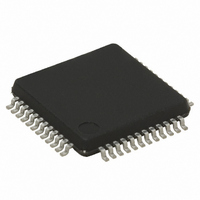
MCU ARM 32BIT 32KB FLASH 48LQFP
Manufacturer
STMicroelectronics
Series
STM32r
Specifications of STM32F103C6T7A
Core Processor
ARM® Cortex-M3™
Core Size
32-Bit
Speed
72MHz
Connectivity
CAN, I²C, IrDA, LIN, SPI, UART/USART, USB
Peripherals
DMA, Motor Control PWM, PDR, POR, PVD, PWM, Temp Sensor, WDT
Number Of I /o
37
Program Memory Size
32KB (32K x 8)
Program Memory Type
FLASH
Ram Size
10K x 8
Voltage - Supply (vcc/vdd)
2 V ~ 3.6 V
Data Converters
A/D 10x12b
Oscillator Type
Internal
Operating Temperature
-40°C ~ 105°C
Package / Case
48-LQFP
Featured Product
STM32 Cortex-M3 Companion Products
Eeprom Size
-
Cpu Family
STM32
Device Core
ARM Cortex-M3
Device Core Size
32b
Frequency (max)
72MHz
Interface Type
CAN/I2C/SPI/USART
Total Internal Ram Size
10KB
# I/os (max)
37
Number Of Timers - General Purpose
3
Operating Supply Voltage (typ)
2.5/3.3V
Operating Supply Voltage (max)
3.6V
Operating Supply Voltage (min)
2V
On-chip Adc
2(10-chx12-bit)
Instruction Set Architecture
RISC
Operating Temp Range
-40C to 105C
Operating Temperature Classification
Industrial
Mounting
Surface Mount
Pin Count
48
Package Type
LQFP
For Use With
497-10048 - BOARD EVAL ACCELEROMETER497-10030 - STARTER KIT FOR STM32KSDKSTM32-PL - KIT IAR KICKSTART STM32 CORTEXM3497-8512 - KIT STARTER FOR STM32F10XE MCU497-8511 - KIT STARTER FOR STM32 512K FLASH497-8505 - KIT STARTER FOR STM32F10XE MCU497-6438 - BOARD EVALUTION FOR STM32 512K497-6289 - KIT PERFORMANCE STICK FOR STM32MCBSTM32UME - BOARD EVAL MCBSTM32 + ULINK-MEMCBSTM32U - BOARD EVAL MCBSTM32 + ULINK2MCBSTM32 - BOARD EVAL FOR STM STM32X SER497-6053 - KIT STARTER FOR STM32497-6052 - KIT STARTER FOR STM32497-6050 - KIT STARTER FOR STM32497-6049 - KIT EVALUATION LOW COST STM32497-6048 - BOARD EVALUATION FOR STM32497-6047 - KIT DEVELOPMENT FOR STM32
Lead Free Status / RoHS Status
Lead free / RoHS Compliant
Eeprom Size
-
Lead Free Status / Rohs Status
Lead free / RoHS Compliant
Available stocks
Company
Part Number
Manufacturer
Quantity
Price
Company:

Part Number:
STM32F103C6T7A
Manufacturer:
ST
Quantity:
1 500
Company:
Part Number:
STM32F103C6T7A
Manufacturer:
STMicroelectronics
Quantity:
10 000
Part Number:
STM32F103C6T7A
Manufacturer:
ST
Quantity:
20 000
Company:
Part Number:
STM32F103C6T7ATR
Manufacturer:
STMicroelectronics
Quantity:
10 000


STM32F103x4, STM32F103x6
List of figures
Figure 1.
Figure 2.
Figure 3.
Figure 4.
Figure 5.
Figure 6.
Figure 7.
Figure 8.
Figure 9.
Figure 10.
Figure 11.
Figure 12.
Figure 13.
Figure 14.
Figure 15.
Figure 16.
Figure 17.
Figure 18.
Figure 19.
Figure 20.
Figure 21.
Figure 22.
Figure 23.
Figure 24.
Figure 25.
Figure 26.
Figure 27.
Figure 28.
Figure 29.
Figure 30.
Figure 31.
Figure 32.
Figure 33.
Figure 34.
Figure 35.
Figure 36.
Figure 37.
Figure 38.
Figure 39.
Figure 40.
Figure 41.
Figure 42.
STM32F103xx performance line block diagram . . . . . . . . . . . . . . . . . . . . . . . . . . . . . . . . . 11
Clock tree . . . . . . . . . . . . . . . . . . . . . . . . . . . . . . . . . . . . . . . . . . . . . . . . . . . . . . . . . . . . . . 12
STM32F103xx performance line LQFP64 pinout . . . . . . . . . . . . . . . . . . . . . . . . . . . . . . . . 21
STM32F103xx performance line TFBGA64 ballout . . . . . . . . . . . . . . . . . . . . . . . . . . . . . . 22
STM32F103xx performance line LQFP48 pinout . . . . . . . . . . . . . . . . . . . . . . . . . . . . . . . . 23
STM32F103xx performance line VFQFPN48 pinout . . . . . . . . . . . . . . . . . . . . . . . . . . . . . 23
STM32F103xx performance line VFQFPN36 pinout . . . . . . . . . . . . . . . . . . . . . . . . . . . . . 24
Memory map . . . . . . . . . . . . . . . . . . . . . . . . . . . . . . . . . . . . . . . . . . . . . . . . . . . . . . . . . . . . 28
Pin loading conditions . . . . . . . . . . . . . . . . . . . . . . . . . . . . . . . . . . . . . . . . . . . . . . . . . . . . . 30
Pin input voltage . . . . . . . . . . . . . . . . . . . . . . . . . . . . . . . . . . . . . . . . . . . . . . . . . . . . . . . . . 30
Power supply scheme. . . . . . . . . . . . . . . . . . . . . . . . . . . . . . . . . . . . . . . . . . . . . . . . . . . . . 30
Current consumption measurement scheme . . . . . . . . . . . . . . . . . . . . . . . . . . . . . . . . . . . 31
Typical current consumption in Run mode versus frequency (at 3.6 V) -
code with data processing running from RAM, peripherals enabled. . . . . . . . . . . . . . . . . . 37
Typical current consumption in Run mode versus frequency (at 3.6 V) -
code with data processing running from RAM, peripherals disabled . . . . . . . . . . . . . . . . . 37
Typical current consumption on V
V
Typical current consumption in Stop mode with regulator in Run mode versus
temperature at V
Typical current consumption in Stop mode with regulator in Low-power mode versus
temperature at V
Typical current consumption in Standby mode versus temperature at
V
High-speed external clock source AC timing diagram . . . . . . . . . . . . . . . . . . . . . . . . . . . . 46
Low-speed external clock source AC timing diagram . . . . . . . . . . . . . . . . . . . . . . . . . . . . . 46
Typical application with an 8 MHz crystal . . . . . . . . . . . . . . . . . . . . . . . . . . . . . . . . . . . . . . 47
Typical application with a 32.768 kHz crystal . . . . . . . . . . . . . . . . . . . . . . . . . . . . . . . . . . . 49
Standard I/O input characteristics - CMOS port . . . . . . . . . . . . . . . . . . . . . . . . . . . . . . . . . 57
Standard I/O input characteristics - TTL port . . . . . . . . . . . . . . . . . . . . . . . . . . . . . . . . . . . 57
5 V tolerant I/O input characteristics - CMOS port . . . . . . . . . . . . . . . . . . . . . . . . . . . . . . . 58
5 V tolerant I/O input characteristics - TTL port . . . . . . . . . . . . . . . . . . . . . . . . . . . . . . . . . 58
I/O AC characteristics definition . . . . . . . . . . . . . . . . . . . . . . . . . . . . . . . . . . . . . . . . . . . . . 61
Recommended NRST pin protection . . . . . . . . . . . . . . . . . . . . . . . . . . . . . . . . . . . . . . . . . 62
I
SPI timing diagram - slave mode and CPHA = 0 . . . . . . . . . . . . . . . . . . . . . . . . . . . . . . . . 66
SPI timing diagram - slave mode and CPHA = 1
SPI timing diagram - master mode
USB timings: definition of data signal rise and fall time . . . . . . . . . . . . . . . . . . . . . . . . . . . 68
ADC accuracy characteristics . . . . . . . . . . . . . . . . . . . . . . . . . . . . . . . . . . . . . . . . . . . . . . . 71
Typical connection diagram using the ADC . . . . . . . . . . . . . . . . . . . . . . . . . . . . . . . . . . . . 72
Power supply and reference decoupling (V
Power supply and reference decoupling(V
VFQFPN36 6 x 6 mm, 0.5 mm pitch, package outline
Recommended footprint (dimensions in mm)
VFQFPN48 7 x 7 mm, 0.5 mm pitch, package outline
Recommended footprint (dimensions in mm)
LQFP64, 10 x 10 mm, 64-pin low-profile quad flat package outline . . . . . . . . . . . . . . . . . . 77
2
BAT
DD
C bus AC waveforms and measurement circuit . . . . . . . . . . . . . . . . . . . . . . . . . . . . . . . . 64
= 3.3 V and 3.6 V . . . . . . . . . . . . . . . . . . . . . . . . . . . . . . . . . . . . . . . . . . . . . . . . . . . . 41
values . . . . . . . . . . . . . . . . . . . . . . . . . . . . . . . . . . . . . . . . . . . . . . . . . . . . . . . . . . . . 39
DD
DD
= 3.3 V and 3.6 V . . . . . . . . . . . . . . . . . . . . . . . . . . . . . . . . . . . . . . . . 40
= 3.3 V and 3.6 V . . . . . . . . . . . . . . . . . . . . . . . . . . . . . . . . . . . . . . . . 40
Doc ID 15060 Rev 5
BAT
(1)
. . . . . . . . . . . . . . . . . . . . . . . . . . . . . . . . . . . . . . . . . 67
with RTC on versus temperature at different
REF+
REF+
(1)(2) . . . . . . . . . . . . . . . . . . . . . . . . . . . . . . . . . . . . . . . . 75
(1)(2) . . . . . . . . . . . . . . . . . . . . . . . . . . . . . . . . . . . . . . . . 76
connected to V
(1)
not connected to V
. . . . . . . . . . . . . . . . . . . . . . . . . . . . . . 66
(1) . . . . . . . . . . . . . . . . . . . . . . . . . . . . . . . . . . 75
(1) . . . . . . . . . . . . . . . . . . . . . . . . . . . . . . . . . . 76
DDA
) . . . . . . . . . . . . . . . . . 73
DDA
). . . . . . . . . . . . . . 72
List of figures
7/87
Related parts for STM32F103C6T7A
Image
Part Number
Description
Manufacturer
Datasheet
Request
R

Part Number:
Description:
STMicroelectronics [RIPPLE-CARRY BINARY COUNTER/DIVIDERS]
Manufacturer:
STMicroelectronics
Datasheet:
Part Number:
Description:
STMicroelectronics [LIQUID-CRYSTAL DISPLAY DRIVERS]
Manufacturer:
STMicroelectronics
Datasheet:

Part Number:
Description:
BOARD EVAL FOR MEMS SENSORS
Manufacturer:
STMicroelectronics
Datasheet:
Part Number:
Description:
NPN TRANSISTOR POWER MODULE
Manufacturer:
STMicroelectronics
Datasheet:
Part Number:
Description:
TURBOSWITCH ULTRA-FAST HIGH VOLTAGE DIODE
Manufacturer:
STMicroelectronics
Datasheet:
Part Number:
Description:
Manufacturer:
STMicroelectronics
Datasheet:
Part Number:
Description:
DIODE / SCR MODULE
Manufacturer:
STMicroelectronics
Datasheet:
Part Number:
Description:
DIODE / SCR MODULE
Manufacturer:
STMicroelectronics
Datasheet:
Part Number:
Description:
Search -----> STE16N100
Manufacturer:
STMicroelectronics
Datasheet:
Part Number:
Description:
Search ---> STE53NA50
Manufacturer:
STMicroelectronics
Datasheet:
Part Number:
Description:
NPN Transistor Power Module
Manufacturer:
STMicroelectronics
Datasheet:
Part Number:
Description:
DIODE / SCR MODULE
Manufacturer:
STMicroelectronics
Datasheet: