Z16F2810FI20EG Zilog, Z16F2810FI20EG Datasheet - Page 13
Z16F2810FI20EG
Manufacturer Part Number
Z16F2810FI20EG
Description
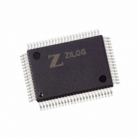
IC ZNEO MCU FLASH 128K 80QFP
Manufacturer
Zilog
Series
Encore!® ZNEOr
Datasheet
1.Z16F2800100ZCOG.pdf
(388 pages)
Specifications of Z16F2810FI20EG
Core Processor
ZNEO
Core Size
16-Bit
Speed
20MHz
Connectivity
I²C, IrDA, LIN, SPI, UART/USART
Peripherals
Brown-out Detect/Reset, DMA, POR, PWM, WDT
Number Of I /o
60
Program Memory Size
128KB (128K x 8)
Program Memory Type
FLASH
Ram Size
4K x 8
Voltage - Supply (vcc/vdd)
2.7 V ~ 3.6 V
Data Converters
A/D 12x10b
Oscillator Type
Internal
Operating Temperature
-40°C ~ 105°C
Package / Case
80-BQFP
Data Bus Width
16 bit
Data Ram Size
4 B
Interface Type
ESPI, I2C, UART
Maximum Clock Frequency
20 MHz
Number Of Programmable I/os
60
Number Of Timers
4
Operating Supply Voltage
2.7 V to 3.6 V
Maximum Operating Temperature
+ 105 C
Mounting Style
SMD/SMT
Minimum Operating Temperature
- 40 C
On-chip Adc
10 bit, 12 Channel
For Use With
770-1003 - ISP 4PORT FOR ZILOG ZNEO MCU269-4537 - DEV KIT FOR Z16F ZNEO
Lead Free Status / RoHS Status
Lead free / RoHS Compliant
Eeprom Size
-
Lead Free Status / Rohs Status
Details
Available stocks
Company
Part Number
Manufacturer
Quantity
Price


PS022008-0810
Option Bits . . . . . . . . . . . . . . . . . . . . . . . . . . . . . . . . . . . . . . . . . . . . . . . . . . . . . . 293
On-Chip Debugger . . . . . . . . . . . . . . . . . . . . . . . . . . . . . . . . . . . . . . . . . . . . . . . . 299
DMA Control Registers . . . . . . . . . . . . . . . . . . . . . . . . . . . . . . . . . . . . . . . . . . 285
DMA Timing . . . . . . . . . . . . . . . . . . . . . . . . . . . . . . . . . . . . . . . . . . . . . . . . . . . 291
Operation . . . . . . . . . . . . . . . . . . . . . . . . . . . . . . . . . . . . . . . . . . . . . . . . . . . . . 293
Option Bit Address Space . . . . . . . . . . . . . . . . . . . . . . . . . . . . . . . . . . . . . . . . 293
Architecture . . . . . . . . . . . . . . . . . . . . . . . . . . . . . . . . . . . . . . . . . . . . . . . . . . . 299
Operation . . . . . . . . . . . . . . . . . . . . . . . . . . . . . . . . . . . . . . . . . . . . . . . . . . . . . 300
DMA Register Description . . . . . . . . . . . . . . . . . . . . . . . . . . . . . . . . . . . . . 269
DMA Control Bit Definitions . . . . . . . . . . . . . . . . . . . . . . . . . . . . . . . . . . . . 271
DMA Water Mark . . . . . . . . . . . . . . . . . . . . . . . . . . . . . . . . . . . . . . . . . . . . 273
DMA Peripheral Interface signals . . . . . . . . . . . . . . . . . . . . . . . . . . . . . . . 273
Buffer Closure . . . . . . . . . . . . . . . . . . . . . . . . . . . . . . . . . . . . . . . . . . . . . . 273
DMA Modes . . . . . . . . . . . . . . . . . . . . . . . . . . . . . . . . . . . . . . . . . . . . . . . . 274
Linked List Mode . . . . . . . . . . . . . . . . . . . . . . . . . . . . . . . . . . . . . . . . . . . . 277
DMA Priority . . . . . . . . . . . . . . . . . . . . . . . . . . . . . . . . . . . . . . . . . . . . . . . 280
DMA Interrupts . . . . . . . . . . . . . . . . . . . . . . . . . . . . . . . . . . . . . . . . . . . . . 281
DMA Request Select Register . . . . . . . . . . . . . . . . . . . . . . . . . . . . . . . . . . 281
DMA Control Register . . . . . . . . . . . . . . . . . . . . . . . . . . . . . . . . . . . . . . . . 285
DMA X transfer Length Register . . . . . . . . . . . . . . . . . . . . . . . . . . . . . . . . 287
DMA Destination Address . . . . . . . . . . . . . . . . . . . . . . . . . . . . . . . . . . . . . 287
DMA Source Address Registers . . . . . . . . . . . . . . . . . . . . . . . . . . . . . . . . 288
DMA List Address Register . . . . . . . . . . . . . . . . . . . . . . . . . . . . . . . . . . . . 289
External DMA Signals . . . . . . . . . . . . . . . . . . . . . . . . . . . . . . . . . . . . . . . . 290
Option Bit Configuration By Reset . . . . . . . . . . . . . . . . . . . . . . . . . . . . . . . 293
Program Memory Address 0000H . . . . . . . . . . . . . . . . . . . . . . . . . . . . . . . 294
Program Memory Address 0001H . . . . . . . . . . . . . . . . . . . . . . . . . . . . . . . 295
Program Memory Address 0002H . . . . . . . . . . . . . . . . . . . . . . . . . . . . . . . 296
Program Memory Address 0003H . . . . . . . . . . . . . . . . . . . . . . . . . . . . . . . 296
Information Area . . . . . . . . . . . . . . . . . . . . . . . . . . . . . . . . . . . . . . . . . . . . 297
IPO Trim registers (Information Area Address 0021H and 0022H) . . . . . . 297
ADC Reference Voltage Trim (Information Area Address 0023H) . . . . . . 298
On-Chip Debug Enable . . . . . . . . . . . . . . . . . . . . . . . . . . . . . . . . . . . . . . . 300
Serial Interface . . . . . . . . . . . . . . . . . . . . . . . . . . . . . . . . . . . . . . . . . . . . . 300
Serial Data Format . . . . . . . . . . . . . . . . . . . . . . . . . . . . . . . . . . . . . . . . . . 301
Baud Rate Generator . . . . . . . . . . . . . . . . . . . . . . . . . . . . . . . . . . . . . . . . 302
P R E L I M I N A R Y
Product Specification
ZNEO
Table of Contents
Z16F Series
xii
Related parts for Z16F2810FI20EG
Image
Part Number
Description
Manufacturer
Datasheet
Request
R

Part Number:
Description:
Communication Controllers, ZILOG INTELLIGENT PERIPHERAL CONTROLLER (ZIP)
Manufacturer:
Zilog, Inc.
Datasheet:

Part Number:
Description:
KIT DEV FOR Z8 ENCORE 16K TO 64K
Manufacturer:
Zilog
Datasheet:

Part Number:
Description:
KIT DEV Z8 ENCORE XP 28-PIN
Manufacturer:
Zilog
Datasheet:

Part Number:
Description:
DEV KIT FOR Z8 ENCORE 8K/4K
Manufacturer:
Zilog
Datasheet:

Part Number:
Description:
KIT DEV Z8 ENCORE XP 28-PIN
Manufacturer:
Zilog
Datasheet:

Part Number:
Description:
DEV KIT FOR Z8 ENCORE 4K TO 8K
Manufacturer:
Zilog
Datasheet:
Part Number:
Description:
CMOS Z8 microcontroller. ROM 16 Kbytes, RAM 256 bytes, speed 16 MHz, 32 lines I/O, 3.0V to 5.5V
Manufacturer:
Zilog, Inc.
Datasheet:
Part Number:
Description:
Low-cost microcontroller. 512 bytes ROM, 61 bytes RAM, 8 MHz
Manufacturer:
Zilog, Inc.
Datasheet:
Part Number:
Description:
Z8 4K OTP Microcontroller
Manufacturer:
Zilog, Inc.
Datasheet:
Part Number:
Description:
CMOS SUPER8 ROMLESS MCU
Manufacturer:
Zilog, Inc.
Datasheet:
Part Number:
Description:
SL1866 CMOSZ8 OTP Microcontroller
Manufacturer:
Zilog, Inc.
Datasheet:
Part Number:
Description:
SL1866 CMOSZ8 OTP Microcontroller
Manufacturer:
Zilog, Inc.
Datasheet:
Part Number:
Description:
OTP (KB) = 1, RAM = 125, Speed = 12, I/O = 14, 8-bit Timers = 2, Comm Interfaces Other Features = Por, LV Protect, Voltage = 4.5-5.5V
Manufacturer:
Zilog, Inc.
Datasheet:
Part Number:
Description:
Manufacturer:
Zilog, Inc.
Datasheet: