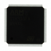
STR911FAW44X6 STMicroelectronics, STR911FAW44X6 Datasheet - Page 54

STR911FAW44X6
Manufacturer Part Number
STR911FAW44X6
Description
MCU 512KB FLASH 96K RAM 128LQFP
Manufacturer
STMicroelectronics
Series
STR9r
Datasheet
1.STEVAL-IFW001V1.pdf
(102 pages)
Specifications of STR911FAW44X6
Core Processor
ARM9
Core Size
32-Bit
Speed
96MHz
Connectivity
CAN, EBI/EMI, I²C, IrDA, Microwire, SPI, SSI, SSP, UART/USART, USB
Peripherals
Brown-out Detect/Reset, DMA, POR, PWM, WDT
Number Of I /o
80
Program Memory Size
512KB (512K x 8)
Program Memory Type
FLASH
Ram Size
96K x 8
Voltage - Supply (vcc/vdd)
1.65 V ~ 2 V
Data Converters
A/D 8x10b
Oscillator Type
Internal
Operating Temperature
-40°C ~ 85°C
Package / Case
128-LQFP
Processor Series
STR911x
Core
ARM966E-S
Data Bus Width
16 bit, 32 bit
Data Ram Size
96 KB
Interface Type
CAN, I2C, IrDA, SSP, UART, USB
Maximum Clock Frequency
96 MHz
Number Of Programmable I/os
80
Number Of Timers
4
Maximum Operating Temperature
+ 85 C
Mounting Style
SMD/SMT
3rd Party Development Tools
EWARM, EWARM-BL, MCBSTR9, MCBSTR9U, MCBSTR9UME, MDK-ARM, RL-ARM, ULINK2
Development Tools By Supplier
STR9-COMSTICK, STR910-EVAL, STR91X-SK/HIT, STR91X-SK/IAR, STR91X-SK/KEI, STR91X-SK/RAI, STR9-DK/RAIS, STR91X-DK/IAR, STX-PRO/RAIS, STR912-D/RAIS, STR79-RVDK/CPP, STR79-RVDKCPP/9, STR79-RVDK, STR79-RVDK/9, STR9-RVDK/BAS, STR79-RVDK/UPG
Minimum Operating Temperature
- 40 C
On-chip Adc
10 bit, 8 Channel
For Use With
MCBSTR9UME - BOARD EVAL MCBSTR9 + ULINK-MEMCBSTR9U - BOARD EVAL MCBSTR9 + ULINK2MCBSTR9 - BOARD EVAL STM STR9 SERIES497-5067 - BOARD EVAL FOR STR910 FAMILY497-5066 - KIT STARTER KEIL FOR STR910497-5065 - KIT STARTER IAR KICKSTART STR912497-5064 - KIT STARTER FOR STR910 FAMILY497-5046 - KIT TOOL FOR ST7/UPSD/STR7 MCU
Lead Free Status / RoHS Status
Lead free / RoHS Compliant
Eeprom Size
-
Lead Free Status / Rohs Status
Details
Other names
497-6281
Available stocks
Company
Part Number
Manufacturer
Quantity
Price
Company:
Part Number:
STR911FAW44X6
Manufacturer:
STMicroelectronics
Quantity:
10 000
Part Number:
STR911FAW44X6
Manufacturer:
ST
Quantity:
20 000
Company:
Part Number:
STR911FAW44X6T
Manufacturer:
STMicroelectronics
Quantity:
10 000
Memory mapping
6
6.1
6.2
54/102
Memory mapping
The ARM966E-S CPU addresses a single linear address space of 4 giga-bytes (2
address 0x0000.0000 to 0xFFFF.FFFF as shown in
from address 0x0000.0000, which is chip-select zero at address zero in the Flash Memory
Interface (FMI).
The Instruction TCM and Data TCM enable high-speed CPU operation without incurring any
performance or power penalties associated with accessing the system buses (AHB and
APB). I-TCM and D-TCM address ranges are shown at the bottom of the memory map in
Figure
Buffered and non-buffered writes
The CPU makes use of write buffers on the AHB and the D-TCM to decouple the CPU from
any wait states associated with a write operation. The user may choose to use write with
buffers on the AHB by setting bit 3 in control register CP15 and selecting the appropriate
AHB address range when writing. By default at reset, buffered writes are disabled (bit 3 of
CP15 is clear) and all AHB writes are non-buffered until enabled.
addressable items on the AHB are aliased at two address ranges, one for buffered writes
and another for non-buffered writes. A buffered write will allow the CPU to continue program
execution while the write-back is performed through a FIFO to the final destination on the
AHB. If the FIFO is full, the CPU is stalled until FIFO space is available. A non-buffered write
will impose an immediate delay to the CPU, but results in a direct write to the final AHB
destination, ensuring data coherency. Read operations from AHB locations are always direct
and never buffered.
System (AHB) and peripheral (APB) buses
The CPU will access SRAM, higher-speed peripherals (USB, Ethernet, Programmable
DMA), and the external bus (EMI) on the AHB at their respective base addresses indicated
in
separate AHB-to-APB bridge units (APB0 and APB1). These bridge units are essentially
address windows connecting the AHB to the APB. To access an individual APB peripheral,
the CPU will place an address on the AHB bus equal to the base address of the appropriate
bridge unit APB0 or APB1, plus the offset of the particular peripheral, plus the offset of the
individual data location within the peripheral.
units APB0 and APB1, and also the base address of each APB peripheral. Please consult
the STR91xFA Reference manual for the address of data locations within each individual
peripheral.
Figure
9.
9. Lower-speed peripherals reside on the APB and are accessed using two
Doc ID 13495 Rev 6
Figure 9
Figure
shows the base addresses of bridge
9. Upon reset the CPU boots
Figure 9
shows that most
STR91xFAxxx
32
) from


