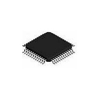
C8051F236-GQR Silicon Laboratories Inc, C8051F236-GQR Datasheet - Page 72

C8051F236-GQR
Manufacturer Part Number
C8051F236-GQR
Description
IC 8051 MCU 8K FLASH 48TQFP
Manufacturer
Silicon Laboratories Inc
Series
C8051F2xxr
Specifications of C8051F236-GQR
Core Processor
8051
Core Size
8-Bit
Speed
25MHz
Connectivity
SPI, UART/USART
Peripherals
Brown-out Detect/Reset, POR, WDT
Number Of I /o
32
Program Memory Size
8KB (8K x 8)
Program Memory Type
FLASH
Ram Size
1.25K x 8
Voltage - Supply (vcc/vdd)
2.7 V ~ 3.6 V
Oscillator Type
Internal
Operating Temperature
-40°C ~ 85°C
Package / Case
48-TQFP, 48-VQFP
Processor Series
C8051F2x
Core
8051
Data Bus Width
8 bit
Data Ram Size
1.25 KB
Interface Type
SPI, UART
Maximum Clock Frequency
25 MHz
Number Of Programmable I/os
32
Number Of Timers
3 bit
Operating Supply Voltage
2.7 V to 3.6 V
Maximum Operating Temperature
+ 85 C
Mounting Style
SMD/SMT
3rd Party Development Tools
PK51, CA51, A51, ULINK2
Development Tools By Supplier
C8051F226DK
Minimum Operating Temperature
- 40 C
On-chip Adc
8 bit, 32 Channel
Lead Free Status / RoHS Status
Lead free / RoHS Compliant
Eeprom Size
-
Data Converters
-
Lead Free Status / Rohs Status
Details
Available stocks
Company
Part Number
Manufacturer
Quantity
Price
Company:
Part Number:
C8051F236-GQR
Manufacturer:
MICROCHIP
Quantity:
2 500
Company:
Part Number:
C8051F236-GQR
Manufacturer:
Silicon Laboratories Inc
Quantity:
10 000
C8051F2xx
72
Bit7:
Bit6:
Bit5:
Bits4–3: RS1–RS0: Register Bank Select.
Bit2:
Bit1:
Bit0:
R/W
CY
Bit7
RS1
CY: Carry Flag.
This bit is set when the last arithmetic operation results in a carry (addition) or a borrow
(subtraction). It is cleared to 0 by all other arithmetic operations.
AC: Auxiliary Carry Flag.
This bit is set when the last arithmetic operation results in a carry into (addition) or a borrow
from (subtraction) the high order nibble. It is cleared to 0 by all other arithmetic operations.
F0: User Flag 0.
This is a bit-addressable, general-purpose flag for use under software control.
These bits select which register bank is used during register accesses.
Note: Any instruction which changes the RS1–RS0 bits must not be immediately followed by
the “MOV Rn, A” instruction.
OV: Overflow Flag.
This bit is set to 1 under the following circumstances:
•An ADD, ADDC, or SUBB instruction causes a sign-change overflow.
•A MUL instruction results in an overflow (result is greater than 255).
•A DIV instruction causes a divide-by-zero condition.
The OV bit is cleared to 0 by the ADD, ADDC, SUBB, MUL, and DIV instructions in all other
cases.
F1: User Flag 1.
This is a bit-addressable, general purpose flag for use under software control.
PARITY: Parity Flag.
This bit is set to 1 if the sum of the eight bits in the accumulator is odd and cleared if the sum
is even.
0
0
1
1
R/W
AC
Bit6
RS0
0
1
0
1
SFR Definition 9.4. PSW: Program Status Word
R/W
Bit5
F0
Register Bank
0
1
2
3
RS1
R/W
Bit4
0x08–0x0F
0x18–0x1F
0x00–0x07
0x10–0x17
Rev. 1.6
Address
RS0
R/W
Bit3
R/W
OV
Bit2
R/W
Bit1
F1
addressable)
PARITY
Bit0
(bit
R
SFR Address:
Reset Value
00000000
0xD0


