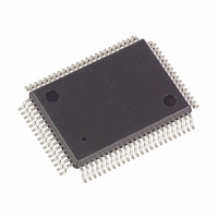
DS5000FP-16+ Maxim Integrated Products, DS5000FP-16+ Datasheet - Page 5

DS5000FP-16+
Manufacturer Part Number
DS5000FP-16+
Description
IC MODULE MICRO 16MHZ 80-QFP
Manufacturer
Maxim Integrated Products
Series
DS500xr
Datasheet
1.DS5000FP-16.pdf
(22 pages)
Specifications of DS5000FP-16+
Core Processor
8051
Core Size
8-Bit
Speed
16MHz
Connectivity
EBI/EMI, SIO, UART/USART
Peripherals
Power-Fail Reset, WDT
Number Of I /o
32
Program Memory Type
SRAM
Ram Size
128 x 8
Voltage - Supply (vcc/vdd)
4.75 V ~ 5.25 V
Oscillator Type
External
Operating Temperature
0°C ~ 70°C
Package / Case
80-MQFP, 80-PQFP
Processor Series
DS5000
Core
8051
Data Bus Width
8 bit
Program Memory Size
8 KB to 64 KB
Data Ram Size
8 KB to 64 KB
Interface Type
3-Wire, RS-232, UART
Maximum Clock Frequency
16 MHz
Number Of Programmable I/os
32
Number Of Timers
2
Operating Supply Voltage
4.75 V to 5.25 V
Maximum Operating Temperature
+ 70 C
Mounting Style
SMD/SMT
Development Tools By Supplier
DS5000TK
Minimum Operating Temperature
0 C
Lead Free Status / RoHS Status
Lead free / RoHS Compliant
Eeprom Size
-
Program Memory Size
-
Data Converters
-
Lead Free Status / Rohs Status
Details
PIN DESCRIPTION (continued)
76, 4, 6, 20, 24,
2, 3, 22, 23, 32,
26, 28, 30, 33,
71, 69, 67, 65,
42, 43, 62, 63,
61, 59, 57, 55
11, 9, 7, 5, 1,
16, 8, 18, 80,
79, 77, 75
13, 14
35, 37
PIN
10
74
78
12
54
72
BD7–BD0
P0.0–P0.7
NAME
BA14–
V
R/W
N.C.
BA0
CE1
CE2
V
V
CCO
CC
LI
General-Purpose I/O Port 0. This port is open-drain and cannot drive a logic 1.
It requires external pullups. Port 0 is also the multiplexed Expanded Address/Data
bus. When used in this mode, it does not require pullups.
Power Supply, +5V
Byte-Wide Address Bus Bits 14–0. This 15-bit bus is combined with the
nonmultiplexed data bus (BD7–BD0) to access NV SRAM. Decoding is
performed on
connect directly to an 8k or 32k SRAM. If an 8k RAM is used, BA13 and BA14
are unconnected. Note: BA13 and BA14 are inverted from the true logical address.
BA14 is lithium backed.
Byte-Wide Data Bus Bits 7–0. This 8-bit bidirectional bus is combined with the
nonmultiplexed address bus (BA14–BA0) to access NV SRAM. Decoding is
performed on
connect directly to an 8k or 32k SRAM, and optionally to a real-time clock.
Read/Write (Active Low). This signal provides the write enable to the SRAMs
on the byte-wide bus. It is controlled by the memory map and partition. The
blocks selected as Program (ROM) is write protected.
Active-Low Chip Enable 1. This is the primary decoded chip enable for memory
access on the byte-wide bus. It connects to the chip enable input of one SRAM.
below V
Active-Low Chip Enable 2. This chip enable is provided to bank switch to a
second block of 32k bytes of nonvolatile data memory. It connects to the chip
enable input of one SRAM or one lithium-backed peripheral such a real-time
clock.
V
V
the level of V
from V
the V
SRAM.
Lithium Voltage Input. Connect to a lithium cell greater than V
greater than V
No Connection. Do not connect.
CE1
CC
CC
falls below V
Output. This is switched between V
is lithium backed. It will remain in a logic high inactive state when V
CCO
CE2
CC
LI
switches to the V
. The lithium cell remains isolated from a load. When V
.
is lithium backed. It will remain in a logic high inactive state when
CC
LImax
CE1
CE1
. When power is above the lithium input, power will be drawn
LI
as shown in the electrical specifications. Nominal value is +3V.
and
and
.
5 of 22
CE2
CE2
LI
. Read/write access is controlled by R/W. BA14–BA0
. Read/write access is controlled by R/W. BD7–BD0
source. V
FUNCTION
CCO
CC
is connected to the V
and V
LI
by internal circuits based on
CC
LImin
CC
pin of an
is below V
and no
CC
falls
LI
,


