PIC16C74/JW Microchip Technology, PIC16C74/JW Datasheet - Page 48
PIC16C74/JW
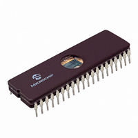
Manufacturer Part Number
PIC16C74/JW
Description
MICRO CTRL 4K 20MHZ EPROM 40CDIP
Manufacturer
Microchip Technology
Series
PIC® 16Cr
Datasheet
1.PIC16C72-04SO.pdf
(289 pages)
Specifications of PIC16C74/JW
Core Processor
PIC
Core Size
8-Bit
Speed
20MHz
Connectivity
I²C, SPI, UART/USART
Peripherals
POR, PWM, WDT
Number Of I /o
33
Program Memory Size
7KB (4K x 14)
Program Memory Type
EPROM, UV
Ram Size
192 x 8
Voltage - Supply (vcc/vdd)
4 V ~ 6 V
Data Converters
A/D 8x8b
Oscillator Type
External
Operating Temperature
0°C ~ 70°C
Package / Case
40-CDIP (0.600", 15.24mm) Window
Lead Free Status / RoHS Status
Contains lead / RoHS non-compliant
Eeprom Size
-
Available stocks
Company
Part Number
Manufacturer
Quantity
Price
Company:

Part Number:
PIC16C74/JW
Manufacturer:
Microchip
Quantity:
29


PIC16C7X
5.3
PORTC is an 8-bit bi-directional port. Each pin is indi-
vidually configurable as an input or output through the
TRISC register. PORTC is multiplexed with several
peripheral functions (Table 5-5). PORTC pins have
Schmitt Trigger input buffers.
When enabling peripheral functions, care should be
taken in defining TRIS bits for each PORTC pin. Some
peripherals override the TRIS bit to make a pin an out-
put, while other peripherals override the TRIS bit to
make a pin an input. Since the TRIS bit override is in
effect while the peripheral is enabled, read-modify-
write instructions (BSF, BCF, XORWF) with TRISC as
destination should be avoided. The user should refer to
the corresponding peripheral section for the correct
TRIS bit settings.
EXAMPLE 5-3:
BCF
BCF
CLRF
BSF
MOVLW
MOVWF
TABLE 5-5:
DS30390E-page 48
Name
RC0/T1OSO/T1CKI
RC1/T1OSI/CCP2
RC2/CCP1
RC3/SCK/SCL
RC4/SDI/SDA
RC5/SDO
RC6/TX/CK
RC7/RX/DT
Legend: ST = Schmitt Trigger input
Note 1: The CCP2 multiplexed function is not enabled on the PIC16C72.
2: The TX/CK and RX/DT multiplexed functions are not enabled on the PIC16C72.
STATUS, RP0
STATUS, RP1
PORTC
STATUS, RP0
0xCF
TRISC
PORTC and TRISC Registers
Applicable Devices
72 73 73A 74 74A 76 77
(2)
(2)
PORTC FUNCTIONS
(1)
INITIALIZING PORTC
Bit#
; Select Bank 0
; PIC16C76/77 only
; Initialize PORTC by
; clearing output
; data latches
; Select Bank 1
; Value used to
; initialize data
; direction
; Set RC<3:0> as inputs
; RC<5:4> as outputs
; RC<7:6> as inputs
bit0
bit1
bit2
bit3
bit4
bit5
bit6
bit7
Buffer Type
ST
ST
ST
ST
ST
ST
ST
ST
Input/output port pin or Timer1 oscillator output/Timer1 clock input
Compare2 output/PWM2 output
output
RC3 can also be the synchronous serial clock for both SPI and I
modes.
RC4 can also be the SPI Data In (SPI mode) or data I/O (I
Synchronous Clock
Synchronous Data
Function
Input/output port pin or Timer1 oscillator input or Capture2 input/
Input/output port pin or Capture1 input/Compare1 output/PWM1
Input/output port pin or Synchronous Serial Port data output
Input/output port pin or USART Asynchronous Transmit, or USART
Input/output port pin or USART Asynchronous Receive, or USART
FIGURE 5-6:
Peripheral Data Out
Data bus
Note 1: I/O pins have diode protection to V
PORT/PERIPHERAL Select
Peripheral input
Peripheral
OE
WR
TRIS
WR
PORT
(3)
2: Port/Peripheral select signal selects between port
3: Peripheral OE (output enable) is only activated if
data and peripheral output.
peripheral select is active.
RD
PORT
TRIS Latch
Data Latch
D
D
RD TRIS
CK
CK
PORTC BLOCK DIAGRAM
(PERIPHERAL OUTPUT
OVERRIDE)
Q
Q
Q
Q
0
1
(2)
1997 Microchip Technology Inc.
Q
EN
D
Schmitt
Trigger
DD
2
V
C mode).
V
N
P
and V
SS
DD
2
I/O
pin
C
SS
(1)
.
Related parts for PIC16C74/JW
Image
Part Number
Description
Manufacturer
Datasheet
Request
R

Part Number:
Description:
IC, 8BIT MCU, PIC16C, 40MHZ, DIP-18
Manufacturer:
Microchip Technology
Datasheet:

Part Number:
Description:
IC, 8BIT MCU, PIC16C, 4MHZ, DIP-28
Manufacturer:
Microchip Technology
Datasheet:
Part Number:
Description:
IC, 8BIT MCU, PIC16C, 4MHZ, DIP-28
Manufacturer:
Microchip Technology
Datasheet:

Part Number:
Description:
IC, 8BIT MCU, PIC16C, 4MHZ, DIP-40
Manufacturer:
Microchip Technology
Datasheet:

Part Number:
Description:
SURFACE MOUNT POWER INDUCTORS
Manufacturer:
RCD [RCD COMPONENTS INC.]
Datasheet:

Part Number:
Description:
Manufacturer:
Microchip Technology Inc.
Datasheet:
Part Number:
Description:
Manufacturer:
Microchip Technology Inc.
Datasheet:
Part Number:
Description:
Manufacturer:
Microchip Technology Inc.
Datasheet:
Part Number:
Description:
Manufacturer:
Microchip Technology Inc.
Datasheet:
Part Number:
Description:
Manufacturer:
Microchip Technology Inc.
Datasheet:
Part Number:
Description:
Manufacturer:
Microchip Technology Inc.
Datasheet: