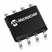
MCP6232-E/MS Microchip Technology, MCP6232-E/MS Datasheet - Page 13

MCP6232-E/MS
Manufacturer Part Number
MCP6232-E/MS
Description
IC OPAMP 1.8V DUAL R-R 8MSOP
Manufacturer
Microchip Technology
Datasheet
1.MCP6231UT-EOT.pdf
(40 pages)
Specifications of MCP6232-E/MS
Slew Rate
0.15 V/µs
Amplifier Type
General Purpose
Number Of Circuits
2
Output Type
Rail-to-Rail
Gain Bandwidth Product
300kHz
Current - Input Bias
1pA
Voltage - Input Offset
5000µV
Current - Supply
20µA
Current - Output / Channel
23mA
Voltage - Supply, Single/dual (±)
1.8 V ~ 6 V
Operating Temperature
-40°C ~ 125°C
Mounting Type
Surface Mount
Package / Case
8-MSOP, Micro8™, 8-uMAX, 8-uSOP,
Op Amp Type
Rail To Rail
No. Of Amplifiers
2
Bandwidth
300kHz
Supply Voltage Range
1.8V To 6V
Amplifier Case Style
MSOP
No. Of Pins
8
Number Of Channels
2
Voltage Gain Db
110 dB
Common Mode Rejection Ratio (min)
61 dB
Input Offset Voltage
5 mV
Operating Supply Voltage
3 V, 5 V
Maximum Operating Temperature
+ 125 C
Mounting Style
SMD/SMT
Minimum Operating Temperature
- 40 C
Lead Free Status / RoHS Status
Lead free / RoHS Compliant
-3db Bandwidth
-
Lead Free Status / Rohs Status
Details
Available stocks
Company
Part Number
Manufacturer
Quantity
Price
Company:
Part Number:
MCP6232-E/MS
Manufacturer:
Microchip
Quantity:
5 941
Part Number:
MCP6232-E/MS
Manufacturer:
MICROCHIP/微芯
Quantity:
20 000
4.6
In applications where low input bias current is critical,
Printed Circuit Board (PCB) surface leakage effects
need to be considered. Surface leakage is caused by
humidity, dust or other contamination on the board.
Under low humidity conditions, a typical resistance
between nearby traces is 10
cause 5 pA of current to flow, which is greater than the
MCP6231/1R/1U/2/4 family’s bias current at +25°C
(1 pA, typical).
The easiest way to reduce surface leakage is to use a
guard ring around sensitive pins (or traces). The guard
ring is biased at the same voltage as the sensitive pin.
An example of this type of layout is shown in
Figure
FIGURE 4-7:
for Inverting Gain.
1.
2.
© 2009 Microchip Technology Inc.
Non-inverting Gain and Unity-Gain Buffer:
a.
b.
Inverting Gain and Transimpedance Amplifiers
(convert current to voltage, such as photo
detectors):
a.
b.
4-7.
PCB Surface Leakage
Connect the non-inverting pin (V
input with a wire that does not touch the
PCB surface.
Connect the guard ring to the inverting input
pin (V
common mode input voltage.
Connect the guard ring to the non-inverting
input pin (V
to the same reference voltage as the op
amp (e.g., V
Connect the inverting pin (V
with a wire that does not touch the PCB
surface.
IN
–). This biases the guard ring to the
V
IN
IN
Guard Ring
DD
+). This biases the guard ring
Example Guard Ring Layout
–
/2 or ground).
12
Ω. A 5V difference would
V
IN
+
IN
–) to the input
IN
V
SS
+) to the
4.7
4.7.1
To minimize the effect of input bias current in an ampli-
fier circuit (this is important for very high source-
impedance applications, such as pH meters and
transimpedance amplifiers), the impedances at the
inverting and non-inverting inputs need to be
matched. This is done by choosing the circuit resistor
values so that the total resistance at each input is the
same.
FIGURE 4-8:
To match the inputs, set all voltage sources to ground
and calculate the total resistance at the input nodes. In
this summing amplifier circuit, the resistance at the
inverting input is calculated by setting V
V
parallel. The total resistance at the inverting input is:
EQUATION 4-1:
At the non-inverting input, V
source. When V
in parallel. The total resistance at the non-inverting
input is:
EQUATION 4-2:
Where:
Where:
OUT
MCP6231/1R/1U/2/4
R
R
VIN –
VIN +
V
V
to ground. In this case, R
Figure 4-8
IN2
IN1
Application Circuits
R
R
X
Y
MATCHING THE IMPEDANCE AT
THE INPUTS
V
R
DD
=
=
R
VIN
R
R
DD
VIN +
G1
G2
shows a summing amplifier circuit.
–
R
is set to ground, both R
total resistance at the inverting
input
total resistance at the inverting
input
=
Z
=
Summing Amplifier Circuit.
----------------------------------------------
⎛
⎝
---------
R
------------------------- -
⎛
⎝
1
G1
----- -
R
1
MCP623X
–
+
X
+
+
1
R
DD
---------
R
----- -
R
F
1
1
G1
1
G2
Y
⎞
⎠
, R
is the only voltage
+
+
DS21881E-page 13
R
----- -
R
G2
1
F
Z
⎞
⎠
and R
IN1
x
V
and R
, V
OUT
F
IN2
are in
y
and
are


