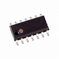
MCP619-I/SL Microchip Technology, MCP619-I/SL Datasheet - Page 16

MCP619-I/SL
Manufacturer Part Number
MCP619-I/SL
Description
IC OPAMP 2.3V QUAD R-R 14SOIC
Manufacturer
Microchip Technology
Specifications of MCP619-I/SL
Slew Rate
0.08 V/µs
Package / Case
14-SOIC (3.9mm Width), 14-SOL
Amplifier Type
General Purpose
Number Of Circuits
4
Output Type
Rail-to-Rail
Gain Bandwidth Product
190kHz
Current - Input Bias
15nA
Voltage - Input Offset
150µV
Current - Supply
19µA
Current - Output / Channel
17mA
Voltage - Supply, Single/dual (±)
2.3 V ~ 5.5 V
Operating Temperature
-40°C ~ 85°C
Mounting Type
Surface Mount
Number Of Channels
4
Common Mode Rejection Ratio (min)
80 dB
Input Offset Voltage
0.15 mV
Input Bias Current (max)
5000 pA
Operating Supply Voltage
3 V, 5 V
Maximum Operating Temperature
+ 85 C
Minimum Operating Temperature
- 40 C
Mounting Style
SMD/SMT
Shutdown
No
Supply Voltage (max)
5.5 V
Supply Voltage (min)
2.3 V
Technology
BiCMOS
Voltage Gain Db
120 dB
Lead Free Status / RoHS Status
Lead free / RoHS Compliant
-3db Bandwidth
-
Lead Free Status / Rohs Status
Lead free / RoHS Compliant
Available stocks
Company
Part Number
Manufacturer
Quantity
Price
Company:
Part Number:
MCP619-I/SL
Manufacturer:
MICROCHIP
Quantity:
12 000
Part Number:
MCP619-I/SL
Manufacturer:
MICROCHIP/微芯
Quantity:
20 000
Company:
Part Number:
MCP619-I/SLG
Manufacturer:
SHINHAN
Quantity:
3 123
MCP616/7/8/9
FIGURE 4-3:
Calculating DC Offset.
To calculate the DC bias point and DC offset, convert
the circuit to its DC equivalent:
• Replace capacitors with open circuits
• Replace inductors with short circuits
• Replace AC voltage sources with short circuits
• Replace AC current sources with open circuits
• Convert DC sources and resistances into their
The DC equivalent circuit for
Figure
FIGURE 4-4:
Now calculate the nominal DC bias point with offset:
DS21613C-page 16
Thevenin equivalent form
V
V
V
EQ
V
1
2
4-4.
1
R
3
R
R
R
V
R
R
EQ
1
4
EQ
EQ
1
C
3
=
=
Example Circuit for
Equivalent DC Circuit.
V
R
2
4
MCP61X
⋅
R
MCP61X
|| R
------------------
R
5
4
R
R
5
+
R
5
Figure 4-3
2
R
2
5
is shown in
V
V
OUT
OUT
EQUATION 4-1:
Use the worst-case specs and source values to
determine the worst-case
offset
input voltage range and output voltage range are not
exceeded.
4.3
There are two specifications that describe the output
swing capability of the MCP616/7/8/9 family of op
amps. The first specification (Maximum Output Voltage
Swing) defines the absolute maximum swing that can
be achieved under the specified load conditions. For
instance, the output voltage swings to within 15 mV of
the negative rail with a 25 kΩ load tied to V
Figure 2-33
when the input goes beyond the linear region of
operation.
The second specification that describes the output
swing capability of these amplifiers is the Linear Output
Voltage
maximum output swing that can be achieved while the
amplifier still operates in its linear region. To verify
linear operation in this range, the large-signal DC
Open-Loop Gain (A
supply rails. The measurement must meet the specified
A
OL
Where:
conditions in the specification table.
V
G
V
V
V
V
V
OOS
for your design. Make sure the common mode
OOS
CM
OUT
I
G
N
CM
OS
OS
I
Rail-to-Rail Output
N
B
=
Range.
= V
= G
= V
1
shows how the output voltage is limited
EQ
+
EQ
N
=
=
=
=
=
=
R
[V
– (I
2
(G
OS
⁄
OL
This
R
B
N
op amp’s noise gain (from the
non-inverting input to the
output)
circuit’s output offset voltage
op amp’s input offset voltage
op amp’s input bias current
op amp’s input offset current
op amp’s coommon mode
input voltage
1
+ I
) is measured at points inside the
+ I
) – V
– I
© 2008 Microchip Technology Inc.
B
OS
OS
output voltage range and
((R
1
specification
((R
/2) R
(G
1
N
1
||R
||R
EQ
– 1) + V
2
) – R
2
) + R
EQ
OOS
EQ
)
defines
) / 2]
DD
the
/2.


