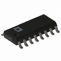
AD605ARZ Analog Devices Inc, AD605ARZ Datasheet - Page 3

AD605ARZ
Manufacturer Part Number
AD605ARZ
Description
IC AMP VGA DUAL LN 40MA 16SOIC
Manufacturer
Analog Devices Inc
Series
X-AMP®r
Type
Variable Gain Amplifierr
Datasheet
1.AD605-EVALZ.pdf
(24 pages)
Specifications of AD605ARZ
Amplifier Type
Variable Gain
Number Of Circuits
2
Slew Rate
170 V/µs
-3db Bandwidth
40MHz
Current - Input Bias
400nA
Current - Supply
18mA
Current - Output / Channel
40mA
Voltage - Supply, Single/dual (±)
4.5 V ~ 5.5 V
Operating Temperature
-40°C ~ 85°C
Mounting Type
Surface Mount
Package / Case
16-SOIC (3.9mm Width)
No. Of Amplifiers
1
Bandwidth
40MHz
Gain Accuracy
1.2dB
No. Of Channels
2
Supply Voltage Range
4.5V To 5.5V
Amplifier Case Style
SOIC
No. Of Pins
16
Number Of Channels
2
Number Of Elements
2
Power Supply Requirement
Single
Common Mode Rejection Ratio
20dB
Voltage Gain Db
34dB
Input Resistance
0.000175@5VMohm
Input Bias Current
0.4@5VnA
Single Supply Voltage (typ)
5V
Dual Supply Voltage (typ)
Not RequiredV
Power Dissipation
90W
Rail/rail I/o Type
No
Single Supply Voltage (min)
4.5V
Single Supply Voltage (max)
5.5V
Dual Supply Voltage (min)
Not RequiredV
Dual Supply Voltage (max)
Not RequiredV
Operating Temp Range
-40C to 85C
Operating Temperature Classification
Industrial
Mounting
Surface Mount
Pin Count
16
Package Type
SOIC N
Lead Free Status / RoHS Status
Lead free / RoHS Compliant
For Use With
AD605-EVALZ - BOARD EVALUATION FOR AD605
Output Type
-
Gain Bandwidth Product
-
Voltage - Input Offset
-
Lead Free Status / Rohs Status
Compliant
Available stocks
Company
Part Number
Manufacturer
Quantity
Price
Part Number:
AD605ARZ
Manufacturer:
ADI/亚德诺
Quantity:
20 000
Company:
Part Number:
AD605ARZ-RL
Manufacturer:
PANASONIC
Quantity:
20 000
SPECIFICATIONS
Each channel @ T
unless otherwise noted.
Table 1.
Parameter
INPUT CHARACTERISTICS
OUTPUT CHARACTERISTICS
ACCURACY
Input Resistance
Input Capacitance
Peak Input Voltage
Input Voltage Noise
Input Current Noise
Noise Figure
Common-Mode Rejection Ratio
−3 dB Bandwidth
Slew Rate
Output Signal Range
Output Impedance
Output Short-Circuit Current
Harmonic Distortion
Two-Tone Intermodulation
1 dB Compression Point
Third-Order Intercept
Channel-to-Channel Crosstalk
Group Delay Variation
VOCM Input Resistance
Absolute Gain Error
Gain Scaling Error
Output Offset Voltage
Output Offset Variation
HD2
HD3
HD2
HD3
Distortion (IMD)
−14 dB to −11 dB
−11 dB to +29 dB
+29 dB to +34 dB
A
= 25°C, V
S
= 5 V, R
Conditions
At minimum gain
VGN = 2.9 V
VGN = 2.9 V
R
R
f = 1 MHz, VGN = 2.65 V
Constant with gain
VGN = 1.5 V, output = 1 V step
R
f = 10 MHz
VGN = 1 V, V
f = 1 MHz
f = 1 MHz
f = 10 MHz
f = 10 MHz
R
f = 1 MHz
f = 10 MHz
f = 10 MHz, VGN = 2.9 V, output referred
f = 10 MHz, VGN = 2.9 V,
V
Ch1: VGN = 2.65 V, inputs shorted,
Ch2: VGN = 1.5 V (mid gain),
f = 1 MHz, V
1 MHz < f < 10 MHz, full gain range
0.25 V < VGN < 0.40 V
0.40 V < VGN < 2.40 V
2.40 V < VGN < 2.65 V
0.4 V < VGN < 2.4 V
V
V
S
S
S
L
OUT
REF
REF
= 50 Ω, f = 10 MHz, VGN = 2.9 V
= 200 Ω, f = 10 MHz, VGN = 2.9 V
= 0 Ω, VGN = 2.9 V, V
≥ 500 Ω
S
= 2.500 V, VOCM = 2.500 V
= 2.500 V, VOCM = 2.500 V
= 1 V p-p, input referred
= 50 Ω, R
OUT
OUT
L
= 1 V p-p
= 1 V p-p
= 500 Ω, C
OUT
= 1 V p-p
Rev. F | Page 3 of 24
L
= 5 pF, V
REF
Min
= 2.5 V (scaling = 20 dB/V), −14 dB to +34 dB gain range,
−1.2
−1.0
−3.5
−30
Typ
175 ± 40
3.0
2.5 ± 2.5
1.8
2.7
8.4
12
−20
40
170
2.5 ± 1.5
2
±40
−64
−68
−51
−53
−72
−60
15
−1
−70
±2.0
45
+1.0
±0.3
−1.25
±0.25
±20
30
AD605A
Max
+3.0
+1.0
+1.2
+30
57
Min
–1.2
–1.0
–3.5
–30
Typ
175 ± 40
3.0
2.5 ± 2.5
1.8
2.7
8.4
12
−20
40
170
2.5 ± 1.5
2
±40
−64
−68
−51
−53
−72
−60
15
−1
−70
±2.0
45
+0.75
±0.2
−1.25
±0.25
±20
30
AD605B
Max
+3.0
+1.0
+1.2
+30
50
AD605
Unit
Ω
pF
V
nV/√Hz
pA/√Hz
dB
dB
dB
MHz
V/μs
V
Ω
mA
dBc
dBc
dBc
dBc
dBc
dBc
dBm
dBm
dB
ns
kΩ
dB
dB
dB
dB/V
mV
mV


