LF351N STMicroelectronics, LF351N Datasheet
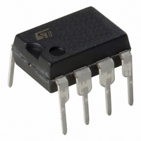
IC OPAMP J-FET SINGLE 8-DIP

LF351N

Manufacturer Part Number
LF351N
Description
IC OPAMP J-FET SINGLE 8-DIP
Manufacturer
STMicroelectronics
Type
General Purpose Amplifierr
Datasheets

Specifications of LF351N

Amplifier Type
J-FET
Number Of Circuits
1
Slew Rate
16 V/µs
Gain Bandwidth Product
4MHz
Current - Input Bias
20pA
Voltage - Input Offset
3000µV
Current - Supply
1.4mA
Current - Output / Channel
40mA
Voltage - Supply, Single/dual (±)
6 V ~ 32 V, ±3 V ~ 16 V
Operating Temperature
0°C ~ 70°C
Mounting Type
Through Hole
Package / Case
8-DIP (0.300", 7.62mm)
Number Of Channels
1
Common Mode Rejection Ratio (min)
70 dB
Input Offset Voltage
10 mV
Input Bias Current (max)
200 pA
Operating Supply Voltage
5 V, 9 V, 12 V
Supply Current
3.4 mA
Maximum Operating Temperature
+ 70 C
Minimum Operating Temperature
0 C
Dual Supply Voltage
+/- 5 V, +/- 9 V, +/- 12 V, +/- 15 V
Maximum Dual Supply Voltage
+/- 16 V
Minimum Dual Supply Voltage
+/- 3 V
Mounting Style
Through Hole
Shutdown
No
Supply Voltage (max)
32 V
Supply Voltage (min)
6 V
Technology
BiFET
Voltage Gain Db
106.02 dB
Bandwidth
4 MHz
Channel Separation
120
Common Mode Rejection Ratio
86
Current, Input Bias
20 pA
Current, Input Offset
5 pA
Current, Offset, Input
5 pA (Typ.)
Current, Output
40 mA
Current, Supply
1.4 mA
Gain Bandwidth
4 MHz (Typ.)
Harmonic Distortion
0.01 %
Input Resistance
10^12 Ohms (Typ.)
Number Of Amplifiers
Single
Package Type
DIP-8
Power Dissipation
680 mW
Resistance, Input
10^12 Ohms
Signal Gain
200 V/mV
Temperature, Operating, Maximum
70 °C
Temperature, Operating, Minimum
0 °C
Temperature, Operating, Range
0 to +70 °C
Time, Rise
0.1 μs
Voltage, Input
±15 V
Voltage, Noise
15 nV/sqrt Hz
Voltage, Offset
3 mV
Voltage, Offset, Input
3 mV (Typ.)
Voltage, Supply
6 to 32 V
Rail/rail I/o Type
No
Number Of Elements
1
Unity Gain Bandwidth Product
4MHz
Input Bias Current
200pA
Single Supply Voltage (typ)
Not RequiredV
Dual Supply Voltage (typ)
±5/±9/±12/±15V
Voltage Gain In Db
106.02dB
Power Supply Requirement
Dual
Shut Down Feature
No
Single Supply Voltage (min)
Not RequiredV
Single Supply Voltage (max)
Not RequiredV
Dual Supply Voltage (min)
±3V
Dual Supply Voltage (max)
±16V
Operating Temp Range
0C to 70C
Operating Temperature Classification
Commercial
Mounting
Through Hole
Pin Count
8
Lead Free Status / RoHS Status
Lead free / RoHS Compliant
Output Type
-
-3db Bandwidth
-
Lead Free Status / Rohs Status
Lead free / RoHS Compliant
Other names
497-2966-5

Available stocks

Company
Part Number
Manufacturer
Quantity
Price
Part Number:
LF351N
Manufacturer:
NSC
Quantity:
1 145
Part Number:
LF351N
Manufacturer:
NSC
Quantity:
31 000
Part Number:
LF351N
Manufacturer:
TI
Quantity:
25
Part Number:
LF351N
Manufacturer:
NS
Quantity:
1 000
Part Number:
LF351N
Manufacturer:
NS
Quantity:
1 000
Part Number:
LF351N
Manufacturer:
NS
Quantity:
9
Part Number:
LF351N
Manufacturer:
ST
Quantity:
20 000
Part Number:
LF351N #T
Manufacturer:
ST
0
Part Number:
LF351N15
Manufacturer:
NS/国半
Quantity:
20 000
Features
Description
These circuits are high speed JFET input single
operational amplifiers incorporating well matched,
high voltage JFET and bipolar transistors in a
monolithic integrated circuit.
The devices feature high slew rates, low input
bias and offset currents, and low offset voltage
temperature coefficient.
April 2008
Internally adjustable input offset voltage
Low power consumption
Wide common-mode (up to V
differential voltage range
Low input bias and offset current
Output short-circuit protection
High input impedance JFET input stage
Internal frequency compensation
Latch up free operation
High slew rate 16 V/µs (typical)
Wide bandwidth single JFET operational amplifiers
CC
+
) and
Rev 2
1 - Offset null 1
2 - Inverting input
3 - Non-inverting input
4 - V
5 - Offset null 2
6 - Output
7 - V
8 - N.C.
(Plastic micro package)
CC
CC
Pin connections
(Plastic package)
-
+
(top view)
SO-8
DIP8
N
D
LF351
www.st.com
1/14
14

Related parts for LF351N

LF351N Summary of contents

Page 1

Wide bandwidth single JFET operational amplifiers Features ■ Internally adjustable input offset voltage ■ Low power consumption ■ Wide common-mode ( differential voltage range ■ Low input bias and offset current ■ Output short-circuit protection ■ High input ...

Page 2

Schematics 1 Schematics Figure 1. Schematic diagram Figure 2. Input offset voltage null circuit 2/ Non-inverting input input Inverting 30k 1.3k 1.3k 35k 35k V CC Offset Null1 Offset Null2 100 W 200 W Output 100 W 8.2k ...

Page 3

LF351 2 Absolute maximum ratings and operating conditions Table 1. Absolute maximum ratings Symbol (1) V Supply voltage CC (2) V Input voltage i V Differential input voltage id Thermal resistance junction to ambient R SO-8 thja DIP8 Thermal resistance ...

Page 4

Electrical characteristics 3 Electrical characteristics Table 3. Electrical characteristics at V Symbol Input offset voltage ( ≤ T ≤ min amb max DV Input offset voltage drift io (1) Input offset current I io ≤ T ...

Page 5

LF351 Figure 3. Maximum peak-to-peak output voltage versus frequency Figure 5. Maximum peak-to-peak output voltage versus frequency Figure 7. Maximum peak-to-peak output voltage versus load resistance Electrical characteristics Figure 4. Maximum peak-to-peak output voltage versus frequency Figure 6. Maximum peak-to-peak ...

Page 6

Electrical characteristics Figure 9. Input bias current versus free air temperature Figure 11. Large signal differential voltage amplification and phase shift versus frequency Figure 13. Supply current per amplifier versus free air temperature 6/14 Figure 10. Large signal differential voltage ...

Page 7

LF351 Figure 15. Common mode rejection ratio versus free air temperature Figure 17. Output voltage versus elapsed time Figure 18. Equivalent input noise voltage Figure 19. Total harmonic distortion versus frequency Electrical characteristics Figure 16. Voltage follower large signal pulse ...

Page 8

Parameter measurement information 4 Parameter measurement information Figure 20. Voltage follower 8/14 Figure 21. Gain-of-10 inverting amplifier LF351 ...

Page 9

LF351 5 Typical application Figure 22. Square wave oscillator (0.5 Hz) Figure 23. High Q notch filter Typical application 9/14 ...

Page 10

... These packages have a lead-free second level interconnect. The category of second level interconnect is marked on the package and on the inner box label, in compliance with JEDEC Standard JESD97. The maximum ratings related to soldering conditions are also marked on the inner box label. ECOPACK is an STMicroelectronics trademark. ECOPACK specifications are available at: www.st.com. 10/14 ...

Page 11

LF351 6.1 DIP8 package information Figure 24. DIP8 package mechanical drawing Table 4. DIP8 package mechanical data Ref Dimensions Millimeters Min. Typ. Max. 5.33 0.38 2.92 3.30 ...

Page 12

Package information 6.2 SO-8 package information Figure 25. SO-8 package mechanical drawing Table 5. SO-8 package mechanical data Ref ccc 12/14 Dimensions Millimeters Min. Typ. Max. 1.75 0.10 ...

Page 13

... SO-8 DIP8 0°C, +70°C SO-8 Revision 1 Initial release. 2 Updated document format. Ordering information Packing Marking Tape LF151N Tape or 151 Tape & reel Tape LF251N Tape or 251 Tape & reel Tape LF351N Tape or 351 Tape & reel Changes 13/14 ...

Page 14

... Information in this document is provided solely in connection with ST products. STMicroelectronics NV and its subsidiaries (“ST”) reserve the right to make changes, corrections, modifications or improvements, to this document, and the products and services described herein at any time, without notice. All ST products are sold pursuant to ST’s terms and conditions of sale. ...

Related keywords