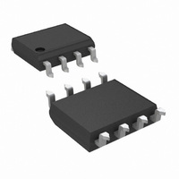
LM7171AIM/NOPB National Semiconductor, LM7171AIM/NOPB Datasheet - Page 5

LM7171AIM/NOPB
Manufacturer Part Number
LM7171AIM/NOPB
Description
IC AMP VERY HI SPD V FDBK 8-SOIC
Manufacturer
National Semiconductor
Series
VIP™ IIIr
Type
Voltage Feedback Amplifierr
Datasheet
1.LM7171BINNOPB.pdf
(20 pages)
Specifications of LM7171AIM/NOPB
Amplifier Type
Voltage Feedback
Number Of Circuits
1
Slew Rate
4100 V/µs
Gain Bandwidth Product
200MHz
-3db Bandwidth
220MHz
Current - Input Bias
2.7µA
Voltage - Input Offset
200µV
Current - Supply
6.5mA
Current - Output / Channel
118mA
Voltage - Supply, Single/dual (±)
5.5 V ~ 36 V, ±2.75 V ~ 18 V
Operating Temperature
-40°C ~ 85°C
Mounting Type
Surface Mount
Package / Case
8-SOIC (3.9mm Width)
Rail/rail I/o Type
No
Number Of Elements
1
Unity Gain Bandwidth Product
125MHz
Common Mode Rejection Ratio
80dB
Input Offset Voltage
1.5mV
Input Bias Current
10uA
Single Supply Voltage (typ)
9/12/15/18/24/28V
Voltage Gain In Db
78dB
Power Supply Rejection Ratio
85dB
Power Supply Requirement
Single/Dual
Shut Down Feature
No
Single Supply Voltage (min)
5.5V
Single Supply Voltage (max)
36V
Dual Supply Voltage (min)
±2.75V
Dual Supply Voltage (max)
±18V
Technology
BiCOM
Operating Temp Range
-40C to 85C
Operating Temperature Classification
Industrial
Mounting
Surface Mount
Pin Count
8
Package Type
SOIC N
Lead Free Status / RoHS Status
Lead free / RoHS Compliant
Output Type
-
Lead Free Status / Rohs Status
RoHS Compliant part
Electrostatic Device
Other names
*LM7171AIM
*LM7171AIM/NOPB
LM7171AIM
*LM7171AIM/NOPB
LM7171AIM
e
i
Symbol
n
8-Pin SOIC
8-Pin MDIP
n
±
Unless otherwise specified, T
Note 1: Absolute Maximum Ratings indicate limits beyond which damage to the device may occur. Operating Ratings indicate conditions for which the device is
intended to be functional, but specific performance is not guaranteed. For guaranteed specifications and the test conditions, see the Electrical Characteristics.
Note 2: Human body model, 1.5 kΩ in series with 100 pF.
Note 3: Applies to both single-supply and split-supply operation. Continuous short circuit operation at elevated ambient temperature can result in exceeding the
maximum allowed junction temperature of 150˚C.
Note 4: The maximum power dissipation is a function of T
(T
Note 5: Typical values represent the most likely parametric norm.
Note 6: All limits are guaranteed by testing or statistical analysis.
Note 7: Large signal voltage gain is the total output swing divided by the input signal required to produce that swing. For V
V
Note 8: The open loop output current is guaranteed, by the measurement of the open loop output voltage swing, using 100Ω output load.
Note 9: Slew Rate is the average of the raising and falling slew rates.
Note 10: Differential gain and phase are measured with A
Note 11: Input differential voltage is applied at V
Note 12: Harmonics are measured with V
Note 13: The THD measurement at low frequency is limited by the test instrument.
Connection Diagram
Ordering Information
OUT
J(MAX)
5V AC Electrical Characteristics
Package
=
–T
±
1V.
A
)/θ
Second Harmonic (Note 12)
Third Harmonic (Note 12)
Input-Referred
Voltage Noise
Input-Referred
Current Noise
JA
. All numbers apply for packages soldered directly into a PC board.
Parameter
J
= 25˚C, V
IN
= 1 V
−40˚C to +85˚C
LM7171AIMX
LM7171BIMX
LM7171AIM
LM7171BIM
LM7171AIN
LM7171BIN
Industrial
S
PP
=
+
, A
±
= +5V, V
15V.
V
f
f
f
f
f = 10 kHz
f = 10 kHz
= +2 and R
IN
IN
IN
IN
V
Temperature Range
J(MAX)
= +2, V
= 10 kHz
= 5 MHz
= 10 kHz
= 5 MHz
−
, θ
Conditions
= −5V, V
IN
JA
L
= 1 V
, and T
= 100Ω.
8-Pin DIP/SO
(Continued)
Top View
PP
A
CM
. The maximum allowable power dissipation at any ambient temperature is P
at 3.58 MHz and both input and output 75Ω terminated.
5
= 0V, and R
−55˚C to +125˚C
(Note 5)
Military
01238502
−102
−110
Typ
−70
−51
L
1.8
14
= 1 kΩ.
LM7171AI
(Note 6)
Limit
S
Tape and Reel
Tape and Reel
=
Transport
±
15V, V
Media
LM7171BI
Rails
Rails
Rails
Rails
(Note 6)
Limit
OUT
=
±
5V. For V
www.national.com
Drawing
Units
dBc
dBc
dBc
dBc
S
M08A
N08E
NSC
=
±
D
5V,
=


