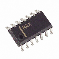
MAX494CSD+ Maxim Integrated Products, MAX494CSD+ Datasheet - Page 12

MAX494CSD+
Manufacturer Part Number
MAX494CSD+
Description
IC OPAMP QUAD R-R 500KHZ 14-SOIC
Manufacturer
Maxim Integrated Products
Datasheet
1.MAX495CPA.pdf
(17 pages)
Specifications of MAX494CSD+
Amplifier Type
General Purpose
Number Of Circuits
4
Output Type
Rail-to-Rail
Slew Rate
0.2 V/µs
Gain Bandwidth Product
500kHz
Current - Input Bias
25nA
Voltage - Input Offset
200µV
Current - Supply
150µA
Current - Output / Channel
30mA
Voltage - Supply, Single/dual (±)
2.7 V ~ 6 V, ±1.35 V ~ 3 V
Operating Temperature
0°C ~ 70°C
Mounting Type
Surface Mount
Package / Case
14-SOIC (3.9mm Width), 14-SOL
Number Of Channels
Quad
Common Mode Rejection Ratio (min)
90 dB
Input Offset Voltage
200 uV
Input Bias Current (max)
60 nA
Supply Current
150 uA
Maximum Power Dissipation
667 mW
Maximum Operating Temperature
+ 70 C
Minimum Operating Temperature
0 C
Mounting Style
SMD/SMT
Supply Voltage (max)
6 V
Supply Voltage (min)
2.7 V
Voltage Gain Db
104 dB
Lead Free Status / RoHS Status
Lead free / RoHS Compliant
-3db Bandwidth
-
Lead Free Status / Rohs Status
Lead free / RoHS Compliant
the op amp in an inverting configuration (Figure 3a);
connect resistor R3 between the noninverting input and
the input signal when using the op amp in a noninvert-
ing configuration (Figure 3b). Select R3 to equal the
parallel combination of R1 and R2. High source resis-
tances will degrade noise performance, due to the ther-
mal noise of the resistor and the input current noise
(which is multiplied by the source resistance).
T
tion circuitry that prevents damage to the precision
input stage from large differential input voltages. This
protection circuitry consists of back-to-back diodes
between IN+ and IN- with two 1.7k
Figure 3a. Reducing Offset Error Due to Bias Current:
Inverting Configuration
Figure 3b. Reducing Offset Error Due to Bias Current:
Noninverting Configuration
he MAX492/MAX494/MAX495 include internal protec-
V
IN
R3 = R2
V
IN
II
R1
Input Stage Protection Circuitry
R1
R3
______________________________________________________________________________________
R3
MAX49_
MAX49_
R2
R3 = R2
Single-Supply Rail-to-Rail Op Amps
II
R1
resistors in series
R2
R1
V
V
Single/Dual/Quad, Micropower,
OUT
OUT
(Figure 4). The diodes limit the differential voltage
applied to the amplifiers’ internal circuitry to no more
than V
(about 0.7V at +25°C).
Input bias current for the ICs (±25nA typical) is speci-
fied for the small differential input voltages. For large
differential input voltages (exceeding V
tion circuitry increases the input current at IN+ and IN-:
For comparator applications requiring large differential
voltages (greater than V
rent that flows through the diodes with external resistors
Figure 4. Input Stage Protection Circuitry
Figure 5. Capacitive-Load Stable Region Sourcing Current
IN+
IN–
Input Current = ———————————
F
10,000
, where V
1000
100
1
1.7k
1.7k
F
is the diodes’ forward-voltage drop
RESISTIVE LOAD (k )
UNSTABLE REGION
(V
F
), you can limit the input cur-
IN
10
+ - V
2 x 1.7k
TO INTERNAL
CIRCUITRY
TO INTERNAL
CIRCUITRY
IN
V
V
R
A
CC
OUT
V
- ) - V
L
TO V
= +1
= +5V
= V
EE
CC
F
F
/2
), this protec-
100
MAX492
MAX494
MAX495
11


