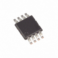
MAX4215EUA+ Maxim Integrated Products, MAX4215EUA+ Datasheet - Page 2

MAX4215EUA+
Manufacturer Part Number
MAX4215EUA+
Description
IC BUFFER R-R W/ENABLE 8-UMAX
Manufacturer
Maxim Integrated Products
Datasheet
1.MAX4222ESD.pdf
(16 pages)
Specifications of MAX4215EUA+
Amplifier Type
Buffer
Number Of Circuits
1
Output Type
Rail-to-Rail
Slew Rate
600 V/µs
-3db Bandwidth
230MHz
Current - Input Bias
5.4µA
Voltage - Input Offset
4000µV
Current - Supply
5.5mA
Current - Output / Channel
120mA
Voltage - Supply, Single/dual (±)
3.15 V ~ 11 V, ±1.575 V ~ 5.5 V
Operating Temperature
-40°C ~ 85°C
Mounting Type
Surface Mount
Package / Case
8-MSOP, Micro8™, 8-uMAX, 8-uSOP,
Lead Free Status / RoHS Status
Lead free / RoHS Compliant
Gain Bandwidth Product
-
ABSOLUTE MAXIMUM RATINGS
Supply Voltage (V
IN_-, IN_+, OUT_, EN_ ....................(V
Output Short-Circuit Duration to V
Continuous Power Dissipation (T
DC ELECTRICAL CHARACTERISTICS
(V
otherwise noted. Typical values are at T
High-Speed, Single-Supply, Gain of 2,
Closed-Loop, Rail-to-Rail Buffers with Enable
Stresses beyond those listed under “Absolute Maximum Ratings” may cause permanent damage to the device. These are stress ratings only, and functional
operation of the device at these or any other conditions beyond those indicated in the operational sections of the specifications is not implied. Exposure to
absolute maximum rating conditions for extended periods may affect device reliability.
2
Operating Supply Voltage
Range
Input Voltage Range
Input Offset Voltage
Input Offset Voltage Drift
Input Offset Voltage
Matching
Input Bias Current
Input Resistance
Voltage Gain
Power-Supply
Rejection Ratio
(Note 2)
Output Resistance
Output Current
Short-Circuit Output
Current
Output Voltage Swing
Disabled Output
Resistance
EN_ Logic Low Threshold
EN_ Logic High Threshold
5-Pin SOT23 (derate 7.1mW/°C above +70°C).............571mW
8-Pin SO (derate 5.9mW/°C above +70°C)...................471mW
CC
_______________________________________________________________________________________
= 5V, V
PARAMETER
EE
= 0, IN_- = 0, EN_ = 5V, R
CC
to V
EE
) ..................................................12V
SYMBOL
R
TCV
OUT(OFF)
PSRR
A
R
V
I
V
CC
V
R
OUT
V
I
V
A
OUT
OUT
I
SC
= +70°C)
OS
B
IN
IN
IH
IL
V
OS
or V
EE
A
EE
- 0.3V) to (V
= +25°C.) (Note 1)
V
IN_+
IN_-
R
Between any two channels for
MAX4217/MAX4219/MAX4222
IN_+
IN_+, over input voltage range
R
V
V
V
f = DC
R
Sinking or sourcing
R
R
R
MAX4215/MAX4219, EN_ = 0, 0
MAX4215/MAX4219
MAX4215/MAX4219
..............Continuous
CC
CC
CC
CC
L
L
L
L
L
L
= 50
= 20 to V
= 50
= 150
= 2k
L
to V
= 5V, V
= 5V, V
= 3.3V, V
50 , (V
=
EE
CC
, guaranteed by PSRR tests
to 0, V
EE
EE
EE
+ 0.3V)
EE
CC
= 0, V
= -5V, V
+ 0.5V)
= 0, V
or V
CONDITIONS
OUT
OUT
EE
OUT
OUT
= V
V
= 2.0V
OUT
SO, QSOP
SOT23-5, µMAX
T
T
V
V
V
V
V
V
Operating Temperature Range ...........................-40°C to +85°C
Storage Temperature Range .............................-65°C to +150°C
Lead Temperature (soldering, 10s) .................................+300°C
= 0.90V
CC
= 0
A
A
CC
OL
CC
OL
CC
OL
8-Pin µMAX (derate 4.1mW/°C above +70°C) .............330mW
14-Pin SO (derate 8.3mW/°C above +70°C)................667mW
16-Pin QSOP (derate 8.3mW/°C above +70°C)...........667mW
= +25°C
= T
/2, noninverting configuration, T
- V
- V
- V
- V
- V
- V
(V
MIN
EE
EE
EE
V
OH
OH
OH
CC
OUT
to T
- 2.0V)
MAX
5V
V
V
V
EE
EE
CC
3.15
MIN
±70
±60
1.9
55
60
- 0.1
- 0.1
- 1.6
A
±120
±150
TYP
1.60
0.04
0.75
0.04
0.06
0.06
5.4
58
66
45
25
= T
4
4
8
1
3
2
1
V
V
V
CC
MIN
CC
CC
- 2.25
- 2.6
+ 0.1
0.075
0.075
MAX
11.0
1.90
1.00
to T
2.1
10
15
12
MAX
UNITS
, unless
µV/°C
M
m
V/V
mA
mA
mV
mV
µA
dB
k
V
V
V
V
V


