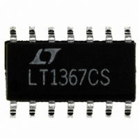
LT1367CS Linear Technology, LT1367CS Datasheet - Page 11

LT1367CS
Manufacturer Part Number
LT1367CS
Description
IC OP-AMP R-R IN/OUT QUAD 14SOIC
Manufacturer
Linear Technology
Datasheet
1.LT1368CN8PBF.pdf
(20 pages)
Specifications of LT1367CS
Amplifier Type
General Purpose
Number Of Circuits
4
Output Type
Rail-to-Rail
Slew Rate
0.13 V/µs
Gain Bandwidth Product
400kHz
Current - Input Bias
10nA
Voltage - Input Offset
200µV
Current - Supply
370µA
Current - Output / Channel
75mA
Voltage - Supply, Single/dual (±)
1.8 V ~ 30 V, ±0.9 V ~ 15 V
Operating Temperature
0°C ~ 70°C
Mounting Type
Surface Mount
Package / Case
14-SOIC (3.9mm Width), 14-SOL
Lead Free Status / RoHS Status
Contains lead / RoHS non-compliant
-3db Bandwidth
-
Available stocks
Company
Part Number
Manufacturer
Quantity
Price
Company:
Part Number:
LT1367CS
Manufacturer:
LT
Quantity:
5 510
Company:
Part Number:
LT1367CS
Manufacturer:
MAXIM
Quantity:
5 510
Part Number:
LT1367CS
Manufacturer:
LINEAR/凌特
Quantity:
20 000
Company:
Part Number:
LT1367CS#PBF
Manufacturer:
LT
Quantity:
1 269
Part Number:
LT1367CS#PBF
Manufacturer:
LINEAR/凌特
Quantity:
20 000
Company:
Part Number:
LT1367CS#TRPBF
Manufacturer:
LINEAR
Quantity:
17 023
Part Number:
LT1367CS#TRPBF
Manufacturer:
LINEAR/凌特
Quantity:
20 000
Typical perForMance characTerisTics
(The data presented here applies to the LT1366/LT1367/LT1368/LT1369 unless otherwise noted.)
applicaTions inForMaTion
Rail-to-Rail Operation
The LT1366 family differs from conventional op amps in the
design of both the input and output stages. Figure 1 shows
a simplified schematic of the amplifier. The input stage
consists of two differential amplifiers, a PNP stage Q1/Q2
and an NPN stage Q3/Q4, which are active over different
– 300mV
0.001
0.01
0.1
1
IN
IN
V
V
V
0.01
+
+
+
–
–
THD + Noise vs Frequency
V
V
R
Q12
S
IN
L
= ±1.5V
= 10k
= 2V
P-P
0.1
Q6
FREQUENCY (kHz)
Q3 Q4
A
V
= 1
V
1
–
D1
A
Q5
V
LT1366 TPC28
= –1
D3
Q1 Q2
10
I
1
Figure 1. LT1366 Simplified Schematic Diagram
D2
Q7
0V
V
+
Large-Signal Response
(LT1366/LT1367)
V
UNITY GAIN
S
Q10
= ±15V
Q8
Q9
Q11
Q13
100µs/DIV
V
portions of the input common mode range. Lateral devices
are used in both input stages, eliminating the need for
clamps across the input pins. Each input stage is trimmed
for offset voltage. A complementary output configuration
(Q23 through Q26) is employed to create an output stage
with rail-to-rail swing. The amplifier is fabricated on Linear
–
C
C
Q14
D7
D4
Q15
LT1366 TPC29
D5
V
+
Q18
Q16
Small-Signal Response
(LT1366/LT1367)
V
UNITY GAIN
LT1366/LT1367
LT1368/LT1369
S
= ±15V
Q17
Q19
Q20
D6
V
V
2µs/DIV
Q21
Q22
+
–
C1
C2
V
V
Q23
Q25
–
+
D7
D8
LT1366 FO1
LT1366 TPC30
Q24
Q26
1366fb
OUT


