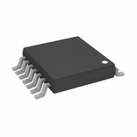
AD8367ARUZ Analog Devices Inc, AD8367ARUZ Datasheet

AD8367ARUZ
Specifications of AD8367ARUZ
Available stocks
Related parts for AD8367ARUZ
AD8367ARUZ Summary of contents
Page 1
FEATURES Broad-range analog variable gain: −2 +42 cutoff frequency of 500 MHz Gain up and gain down modes Linear-in-dB, scaled 20 mV/dB Resistive ground referenced input Nominal Z = 200 Ω IN On-chip, square-law detector ...
Page 2
AD8367 TABLE OF CONTENTS Features .............................................................................................. 1 Applications....................................................................................... 1 Functional Block Diagram .............................................................. 1 General Description ......................................................................... 1 Revision History ............................................................................... 2 Specifications..................................................................................... 3 Absolute Maximum Ratings............................................................ 5 ESD Caution.................................................................................. 5 Pin Configuration and Function Descriptions............................. 6 Typical Performance Characteristics ...
Page 3
SPECIFICATIONS 25°C, system impedance Table 1. Parameter OVERALL FUNCTION Frequency Range GAIN Range INPUT STAGE Maximum Input Input Resistance GAIN CONTROL INTERFACE Scaling Factor Gain Law Conformance Maximum Gain Minimum Gain ...
Page 4
AD8367 Parameter f = 140 MHz Gain Gain Scaling Factor Gain Intercept Noise Figure Output IP3 Output 1 dB Compression Point f = 190 MHz Gain Gain Scaling Factor Gain Intercept Noise Figure Output IP3 Output 1 dB Compression Point ...
Page 5
ABSOLUTE MAXIMUM RATINGS Table 2. Parameter Supply Voltage VPSO, VPSI ENBL Voltage MODE Select Voltage V Control Voltage GAIN Input Voltage Internal Power Dissipation θ JA Maximum Junction Temperature Operating Temperature Range Storage Temperature Range Lead Temperature Range (Soldering 60 ...
Page 6
AD8367 PIN CONFIGURATION AND FUNCTION DESCRIPTIONS Table 3. Pin Function Descriptions Pin No. Mnemonic Description ICOM Signal Common. Connect to low impedance ground. 2 ENBL A HI Activates the Device. 3 INPT Signal Input. 200 Ω to ...
Page 7
TYPICAL PERFORMANCE CHARACTERISTICS 25°C, system impedance 0.9V 40 0.8V 0.7V 30 0.6V 0.5V 20 0.4V 0.3V 10 0.2V 0.1V 0 –10 10 100 FREQUENCY (MHz) Figure 3. Gain vs. ...
Page 8
AD8367 100 FREQUENCY (MHz) Figure 9. OIP3 vs. Frequency for –2 –4 –6 –8 0 0.1 0.2 0.3 0.4 0.5 0.6 V (V) GAIN Figure 10. Output P1dB ...
Page 9
FREQUENCY (MHz) Figure 15. Input Resistance and Series Reactance vs. Frequency 500 mV GAIN 90 120 150 180 300mV 210 500mV 700mV 240 270 Figure 16. Input ...
Page 10
AD8367 1.0 0.9 0.8 140MHz 70MHz 0.7 0.6 0.5 240MHz 0.4 10MHz 0.3 0.2 0.1 0 –60 –50 –40 –30 –20 INPUT LEVEL (dBV rms) Figure 21. AGC RSSI (Voltage on DETO Pin) vs. Input Power at 10 MHz, 70 ...
Page 11
THEORY OF OPERATION The AD8367 is a variable gain, single-ended, IF amplifier based on Analog Devices’ patented X-AMP architecture. It offers accurate gain control with span and bandwidth of 500 MHz. It can be ...
Page 12
AD8367 V B1 FROM INTEGRATOR V B2 Figure 29 Ω resistor is added to the output to prevent package resonance. POWER AND VOLTAGE METRICS Although power is the traditional metric used in the analysis of cascaded systems, most ...
Page 13
RMS DETECTION The AD8367 contains a square-law detector that senses the output signal and compares calibrated setpoint of 354 mV rms, which corresponds p-p sine wave. This setpoint is internally set and cannot ...
Page 14
AD8367 APPLICATIONS The AD8367 can be configured either as a VGA whose gain is controlled externally through the GAIN pin AGC amplifier, using a supply voltage of 2 5.5 V. The supply to the VPSO ...
Page 15
VGA OPERATION The AD8367 is a general-purpose VGA suitable for use in a wide variety of applications where voltage control of gain is needed. While having a 500 MHz bandwidth, its use is not limited to high frequency signal processing. ...
Page 16
AD8367 held to within 0 the setpoint for >35 dB range of input levels. The dynamics of this loop are controlled by C conjunction with an on-chip equivalent resistance kΩ which form an effective time-constant T ...
Page 17
J1 10nF INPUT R6 57.6Ω 10kΩ Note that in this circuit the AD8367’s MODE pin must be pulled high to obtain correct feedback polarity because the integrator inverts the polarity of the feedback signal. The relationship between ...
Page 18
AD8367 –20 –25 –30 –35 –40 380MHz –45 –50 10MHz –55 –60 –20 –15 –10 –5 POUT (dBm INTO 200Ω) Figure 40. ACPR vs. Output Power for QPSK Waveform (QPSK: 4.096 MS/s; α = 0.22; 1 User) Table 6. Suggested ...
Page 19
EVALUATION BOARD Figure 42 shows the schematic of the AD8367 evaluation board. The board is powered by a single supply of 2 5.5 V. TP3 MODE J1 INPUT R1 57.6Ω GAIN Figure 43. Layout of Component Side R7 ...
Page 20
AD8367 Table 7 details the various configuration options of the evaluation board. Table 7. Evaluation Board Configuration Options Component Function TP1, TP2 Supply and Ground Vector Pins. TP3, TP4 Mode and Gain Vector Pins. SW1 VGA/AGC Select: Used to select ...
Page 21
... PIN 1 1.05 1.00 0.80 ORDERING GUIDE Model Temperature Range AD8367ARU −40°C to +85°C AD8367ARU-REEL-7 −40°C to +85°C 1 AD8367ARUZ −40°C to +85°C AD8367ARUZ-RL7 1 −40°C to +85°C AD8367-EVAL Pb-free part. 5.10 5.00 4. 6.40 BSC 1 7 0.65 BSC ...
Page 22
AD8367 NOTES Rev Page ...
Page 23
NOTES Rev Page AD8367 ...
Page 24
AD8367 NOTES © 2005 Analog Devices, Inc. All rights reserved. Trademarks and registered trademarks are the property of their respective owners. C02710–0–7/05(A) Rev Page ...


