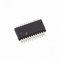
EL5373IUZ-T7 Intersil, EL5373IUZ-T7 Datasheet - Page 11

EL5373IUZ-T7
Manufacturer Part Number
EL5373IUZ-T7
Description
IC DRIVER TRIPLE 450MHZ 24-QSOP
Manufacturer
Intersil
Datasheet
1.EL5173ISZ-T7.pdf
(14 pages)
Specifications of EL5373IUZ-T7
Amplifier Type
Differential
Number Of Circuits
3
Output Type
Differential
Slew Rate
1100 V/µs
-3db Bandwidth
450MHz
Current - Input Bias
13µA
Voltage - Input Offset
3000µV
Current - Supply
12mA
Current - Output / Channel
50mA
Voltage - Supply, Single/dual (±)
4.75 V ~ 11 V, ±2.38 V ~ 5.5 V
Operating Temperature
-40°C ~ 85°C
Mounting Type
Surface Mount
Package / Case
24-QSOP
Lead Free Status / RoHS Status
Lead free / RoHS Compliant
Gain Bandwidth Product
-
Available stocks
Company
Part Number
Manufacturer
Quantity
Price
Company:
Part Number:
EL5373IUZ-T7
Manufacturer:
Intersil
Quantity:
1 000
By setting the two PD
can solve the output current and R
overheat.
Power Supply Bypassing and Printed Circuit
Board Layout
As with any high frequency device, a good printed circuit
board layout is necessary for optimum performance. Lead
lengths should be as short as possible. The power supply
pin must be well bypassed to reduce the risk of oscillation.
For normal single supply operation, where the V
connected to the ground plane, a single 4.7µF tantalum
capacitor in parallel with a 0.1µF ceramic capacitor from V
to GND will suffice. This same capacitor combination should
be placed at each supply pin to ground if split supplies are to
be used. In this case, the V
supply rail.
Typical Applications
MAX
equations equal to each other, we
EL5173/
EL5373
S
- pin becomes the negative
11
LOAD
to avoid the device
FIGURE 25. TWISTED PAIR CABLE DRIVER
50
50
S
- pin is
EL5173, EL5373
Z
O
S
= 100Ω
+
For good AC performance, parasitic capacitance should be
kept to minimum. Use of wire-wound resistors should be
avoided because of their additional series inductance. Use
of sockets should also be avoided if possible. Sockets add
parasitic inductance and capacitance that can result in
compromised performance. Minimizing parasitic capacitance
at the amplifier’s inverting input pin is very important. The
feedback resistor should be placed very close to the
inverting input pin. Strip line design techniques are
recommended for the signal traces.
50Ω
50Ω
V
V
V
V
FB
IN
INB
REF
EL5175/
EL5375
0Ω
V
OUT
September 14, 2010
FN7312.8


