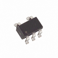
MAX4014EUK+T Maxim Integrated Products, MAX4014EUK+T Datasheet - Page 9

MAX4014EUK+T
Manufacturer Part Number
MAX4014EUK+T
Description
IC BUFFER R-R SOT23-5
Manufacturer
Maxim Integrated Products
Datasheet
1.MAX4019ESD.pdf
(12 pages)
Specifications of MAX4014EUK+T
Amplifier Type
Buffer
Number Of Circuits
1
Output Type
Rail-to-Rail
Slew Rate
600 V/µs
-3db Bandwidth
200MHz
Current - Input Bias
5.4µA
Voltage - Input Offset
4000µV
Current - Supply
5.5mA
Current - Output / Channel
120mA
Voltage - Supply, Single/dual (±)
3.15 V ~ 11 V, ±1.575 V ~ 5.5 V
Operating Temperature
-40°C ~ 85°C
Mounting Type
Surface Mount
Package / Case
SOT-23-5, SC-74A, SOT-25
Number Of Channels
1
Voltage Gain Db
6.02 dB
Input Offset Voltage
4 mV
Operating Supply Voltage
5 V, 9 V
Maximum Power Dissipation
571 mW
Maximum Operating Temperature
+ 85 C
Mounting Style
SMD/SMT
Maximum Dual Supply Voltage
+/- 5.5 V
Minimum Operating Temperature
- 40 C
Lead Free Status / RoHS Status
Lead free / RoHS Compliant
Gain Bandwidth Product
-
Lead Free Status / Rohs Status
Details
The input range for the MAX4014 family extends from
(V
increases the dynamic range for single-supply applica-
tions. The outputs drive a 2kΩ load to within 60mV of
the power-suply rails. With heavier loads, the output
swing is reduced as shown in the Electrical Character-
istics and the Typical Operating Characteristics. As the
load increases, the input range is effectively limited by
Figure 2. Enable Logic-Low Input Current vs. Enable Logic-
Low Threshold
Figure 3. Circuit to Reduce Enable Logic-Low Input Current
EE
Low-Cost, High-Speed, Single-Supply, Gain of +2
Input Voltage Range and Output Swing
- 100mV) to (V
-100
-120
-140
-160
-20
-40
-60
-80
IN+
IN-
20
0
0
Buffers with Rail-to-Rail Outputs in SOT23
500Ω
_______________________________________________________________________________________
100
CC
- 2.25V). Input ground sensing
V
IL
200
(mV ABOVE V
MAX40_ _
ENABLE
500Ω
300
EN_
10k
EE
)
400
OUT
500
the output-drive capability, since the buffers have a
fixed voltage gain of +2 or -1.
For example, a 50Ω load can typically be driven from
40mV above V
when operating from a single +5V supply. If the buffer is
operated in the noninverting, gain of +2 configuration
with the inverting input grounded, the effective input
voltage range becomes 20mV to 1.7V, instead of the
-100mV to 2.75V indicated by the Electrical Character-
istics. Beyond the effective input range, the buffer out-
put is a nonlinear function of the input, but it will not
undergo phase reversal or latchup.
The MAX4019 has an enable feature (EN_) that allows
the buffer to be placed in a low-power state. When the
buffers are disabled, the supply current will not exceed
550µA per buffer.
As the voltage at the EN_ pin approaches the negative
supply rail, the EN_ input current rises. Figure 2 shows
a graph of EN_ input current versus EN_ pin voltage.
Figure 3 shows the addition of an optional resistor in
series with the EN pin, to limit the magnitude of the cur-
rent increase. Figure 4 displays the resulting EN pin
input current to voltage relationship.
Figure 4. Enable Logic-Low Input Current vs. Enable Logic-
Low Threshold with 10kΩ Series Resistor
-10
-1
-2
-3
-4
-5
-6
-7
-8
-9
0
EE
0
to 1.6V below V
100
V
IL
200
(mV ABOVE V
300
CC
EE
)
, or 40mV to 3.4V
400
500
Enable
9


