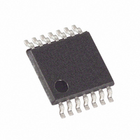
MAX4478AUD+ Maxim Integrated Products, MAX4478AUD+ Datasheet - Page 4

MAX4478AUD+
Manufacturer Part Number
MAX4478AUD+
Description
IC OP AMP R-R LN 10MHZ 14-TSSOP
Manufacturer
Maxim Integrated Products
Datasheet
1.MAX4477AUA.pdf
(21 pages)
Specifications of MAX4478AUD+
Amplifier Type
General Purpose
Number Of Circuits
4
Output Type
Rail-to-Rail
Slew Rate
3 V/µs
Gain Bandwidth Product
10MHz
Current - Input Bias
1pA
Voltage - Input Offset
70µV
Current - Supply
2.5mA
Current - Output / Channel
48mA
Voltage - Supply, Single/dual (±)
2.7 V ~ 5.5 V, ±1.35 V ~ 2.75 V
Operating Temperature
-40°C ~ 125°C
Mounting Type
Surface Mount
Package / Case
14-TSSOP
Number Of Channels
4
Common Mode Rejection Ratio (min)
90 dB
Input Offset Voltage
0.35 mV
Input Bias Current (max)
150 pA
Operating Supply Voltage
3 V, 5 V
Maximum Power Dissipation
727 mW
Maximum Operating Temperature
+ 125 C
Minimum Operating Temperature
- 40 C
Mounting Style
SMD/SMT
Shutdown
No
Supply Voltage (max)
5.5 V
Supply Voltage (min)
2.7 V
Technology
BiCMOS
Voltage Gain Db
120 dB
Lead Free Status / RoHS Status
Lead free / RoHS Compliant
-3db Bandwidth
-
Lead Free Status / Rohs Status
Lead free / RoHS Compliant
AC ELECTRICAL CHARACTERISTICS (continued)
(V
SOT23, Low-Noise, Low-Distortion,
Wide-Band, Rail-to-Rail Op Amps
Note 1: All devices are 100% tested at T
Note 2: SHDN is available on the MAX4475/MAX4488 only.
Note 3: Guaranteed by the PSRR test.
Note 4: Guaranteed by design.
Note 5: Full-power bandwidth for unity-gain stable devices (MAX4475–MAX4478) is measured in a closed-loop gain of +2V/V to
Note 6: Lowpass-filter bandwidth is 22kHz for f = 1kHz and 80kHz for f = 20kHz. Noise floor of test equipment = 10nV/√Hz.
(V
measurements, T
4
Total Harmonic Distortion Plus
Noise (Note 6)
Capacitive-Load Stability
Gain Margin
Phase Margin
Settling Time
Delay Time to Shutdown
Enable Delay Time from Shutdown
Power-Up Delay Time
DD
DD
18
16
14
12
10
_______________________________________________________________________________________
8
6
4
2
0
= +5V, V
= +5V, V
INPUT OFFSET VOLTAGE DISTRIBUTION
-50
accommodate the input voltage range, V
-40
PARAMETER
-30 -20
SS
SS
= 0V, V
= 0V, V
A
-10 0 10 20 30 40 50
= +25°C, unless otherwise noted.)
V
OS
(µV)
CM
CM
= 0V, V
= 0V, V
OUT
OUT
SYMBOL
THD + N
= V
= V
GM
ΦM
t
t
A
SH
EN
= +25°C. Limits over temperature are guaranteed by design.
DD
DD
/2, R
/2, R
-100
-150
-200
-250
250
200
150
100
-50
OUT
V
A
(MAX4488/MAX4489),
R
No sustained oscillations
MAX4475–MAX4478, A
MAX4488/MAX4489, A
To 0.01%, V
V
V
50
L
0
L
OUT
OUT
DD
V
L
-50
tied to V
tied to V
= +5V/V
= 1kΩ to GND
OFFSET VOLTAGE vs. TEMPERATURE
= 4V
= 0 to 5V step, V
V
COM
= 2V
= 2.5V, V
-25
= 0V
P-P
P-P
DD
DD
.
OUT
0
TEMPERATURE (°C)
/2, SHDN = V
,
/2, input noise floor of test equipment =10nV/√Hz for all distortion
CONDITIONS
OUT
= 2V step
25
settles to 0.1%
Typical Operating Characteristics
OUT
50
V
V
= +5V/V
= +1V/V
f = 1kHz
f = 20kHz
stable to 0.1%
75
DD
, T
100
A
= +25°C.)
125
50
40
30
20
10
MIN
0
-0.5
vs. INPUT COMMON-MODE VOLTAGE
INPUT COMMON-MODE VOLTAGE (V)
0.5
INPUT OFFSET VOLTAGE
0.0005
0.008
V
TYP
200
DD
1.5
12
70
80
10
13
2
= 3V
1.5
MAX
2.5
V
DD
= 5V
degrees
3.5
UNITS
dB
pF
µs
µs
µs
µs
%
4.5


