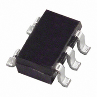
AD8091ART-R2 Analog Devices Inc, AD8091ART-R2 Datasheet - Page 7

AD8091ART-R2
Manufacturer Part Number
AD8091ART-R2
Description
IC OPAMP VF R-R LDIST LP SOT23-5
Manufacturer
Analog Devices Inc
Datasheet
1.AD8091ARTZ-R7.pdf
(20 pages)
Specifications of AD8091ART-R2
Rohs Status
RoHS non-compliant
Amplifier Type
Voltage Feedback
Number Of Circuits
1
Output Type
Rail-to-Rail
Slew Rate
170 V/µs
-3db Bandwidth
110MHz
Current - Input Bias
1.4µA
Voltage - Input Offset
1800µV
Current - Supply
4.8mA
Current - Output / Channel
45mA
Voltage - Supply, Single/dual (±)
3 V ~ 12 V, ±1.5 V ~ 6 V
Operating Temperature
-40°C ~ 85°C
Mounting Type
Surface Mount
Package / Case
SOT-23-5, SC-74A, SOT-25
Gain Bandwidth Product
-
MAXIMUM POWER DISSIPATION
The maximum safe power dissipation in the AD8091/AD8092
package is limited by the associated rise in junction temperature
(T
the junction temperature. At approximately 150°C, which is the
glass transition temperature, the plastic changes its properties.
Even temporarily exceeding this temperature limit may change
the stresses that the package exerts on the die, permanently
shifting the parametric performance of the AD8091/AD8092.
Exceeding a junction temperature of 175°C for an extended
period of time can result in changes in the silicon devices,
potentially causing failure.
The still-air thermal properties of the package (θ
temperature (T
(P
The junction temperature can be calculated as
The power dissipated in the package (P
quiescent power dissipation and the power dissipated in the
package due to the load drive for all outputs. The quiescent
power is the voltage between the supply pins (V
quiescent current (I
to midsupply, then the total drive power is V
which is dissipated in the package and some in the load
(V
the load power is the drive power dissipated in the package.
RMS output voltages should be considered. If R
−V
V
S
D
J
OUT
) on the die. The plastic encapsulating the die locally reaches
× I
) can be used to determine the junction temperature of the die.
S
, as in single-supply operation, then the total drive power is
T
P
P
OUT
× I
J
D
D
=
=
=
.
OUT
T
quiescent
(
A
V
). The difference between the total drive power and
S
+
×
A
(
), and the total power dissipated in the package
P
I
D
S
×
)
S
power
+
θ
). Assuming that the load (R
JA
⎛
⎜
⎜
⎝
)
⎛
⎜ ⎜
⎝
V
2
S
+
×
(
total
V
R
OUT
L
drive
⎞
⎟ ⎟
⎠
−
D
⎛
⎜
⎜
⎝
) is the sum of the
power
V
OUT
R
L
S
/2 × I
2
JA
⎞
⎟
⎟
⎠
−
), the ambient
L
S
⎞
⎟
⎟
⎠
) times the
L
is referenced to
load
) is referenced
OUT
, some of
power
)
Rev. C | Page 7 of 20
If the rms signal levels are indeterminate, then consider the
worst case when V
In single-supply operation with R
case is V
Airflow increases heat dissipation, effectively reducing θ
more metal directly in contact with the package leads from
metal traces, through holes, ground, and power planes reduces
the θ
at the input leads of high speed op amps as discussed in the
Input Capacitance section.
Figure 4 shows the maximum safe power dissipation in the
package vs. the ambient temperature for the SOIC-8
(125°C/W), SOT23-5 (180°C/W), and MSOP-8 (150°C/W) on a
JEDEC standard four-layer board.
JA
P
. Care must be taken to minimize parasitic capacitances
D
2.0
1.5
1.0
0.5
=
OUT
0
–40 –30 –20 –10
(
V
T
= V
S
J
= 150°C
×
Figure 4. Maximum Power Dissipation vs.
I
S
/2.
S
Temperature for a Four-Layer Board
)
OUT
MSOP-8
+
SOIC-8
⎛
⎜
⎝
= V
AMBIENT TEMPERATURE (°C)
V
R
4
SOT23-5
S
L
0
⎞
⎟
⎠
S
/4 for R
2
10
20
L
L
referenced to −V
30
to midsupply
AD8091/AD8092
40
50
60
70
S
, the worst
80
JA
90
. Also,


