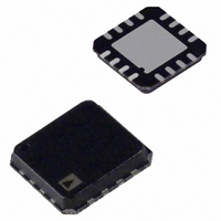
AD8555ACP-REEL7 Analog Devices Inc, AD8555ACP-REEL7 Datasheet - Page 20

AD8555ACP-REEL7
Manufacturer Part Number
AD8555ACP-REEL7
Description
IC AMP CHOPPER 2MHZ 10MA 16LFCSP
Manufacturer
Analog Devices Inc
Series
DigiTrim®r
Datasheet
1.AD8555ARZ.pdf
(28 pages)
Specifications of AD8555ACP-REEL7
Rohs Status
RoHS non-compliant
Amplifier Type
Chopper (Zero-Drift)
Number Of Circuits
1
Slew Rate
1.2 V/µs
Gain Bandwidth Product
2MHz
Current - Input Bias
16nA
Voltage - Input Offset
2µV
Current - Supply
2mA
Current - Output / Channel
10mA
Voltage - Supply, Single/dual (±)
2.7 V ~ 5.5 V
Operating Temperature
-40°C ~ 125°C
Mounting Type
Surface Mount
Package / Case
16-LFCSP
Output Type
-
-3db Bandwidth
-
AD8555
Table 10. Timing Specifications
Timing Parameter
t
t
t
Table 11. 38-Bit Serial Word Format
Field No.
Field 0
Field 1
Field 2
Field 3
Field 4
Field 5
A 38-bit serial word is used, divided into 6 fields. Assuming
each bit can be loaded in 60 μs, the 38-bit serial word transfers
in 2.3 ms. Table 11 summarizes the word format.
w0
w1
ws
WAVEFORM
CODE
t
Bits
Bits 0 to 11
Bits 12 to 13
Bits 14 to 15
Bits 16 to 17
Bits 18 to 25
Bits 26 to 37
W0
0
t
WS
Description
Pulse Width for Loading 0 into Shift Register
Pulse Width for Loading 1 into Shift Register
Width between Pulses
t
W1
1
Description
12-Bit Start of Packet 1000 0000 0001
2-Bit Function
2-Bit Parameter
2-Bit Dummy 10
8-Bit Value
12-Bit End of Packet 0111 1111 1110
00: Change Sense Current
01: Simulate Parameter Value
10: Program Parameter Value
11: Read Parameter Value
00: Second Stage Gain Code
01: First Stage Gain Code
10: Output Offset Code
11: Other Functions
Parameter 00 (Second Stage Gain Code): 3 LSBs Used
Parameter 01 (First Stage Gain Code): 7 LSBs Used
Parameter 10 (Output Offset Code): All 8 Bits Used
Parameter 11 (Other Functions)
Bit 0 (LSB): Master Fuse
Bit 1: Fuse for Production Test at Analog Devices
Bit 2: Parity Fuse
Figure 51. Timing Diagram for Code 010011
t
WS
t
W0
0
Rev. A | Page 20 of 28
t
WS
t
W0
0
t
WS
Fields 0 and 5 are the start of packet and end of packet field,
respectively. Matching the start of packet field with 1000 0000
0001 and the end of packet field with 0111 1111 1110 ensures
that the serial word is valid and enables decoding of the other
fields. Field 3 breaks up the data and ensures that no data com-
bination can inadvertently trigger the start of packet and end of
packet fields. Field 0 should be written first and Field 5 written
last. Within each field, the MSB must be written first and the
LSB written last. The shift register features power-on reset to
minimize the risk of inadvertent programming; power-on reset
occurs when VDD is between 0.7 V and 2.2 V.
t
W1
1
t
WS
Specification
Between 50 ns and 10 μs
≥50 μs
≥10 μs
t
W1
1


