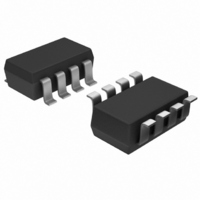
MAX6368HKA31+T Maxim Integrated Products, MAX6368HKA31+T Datasheet - Page 8

MAX6368HKA31+T
Manufacturer Part Number
MAX6368HKA31+T
Description
IC SUPERVISOR MPU LP SOT23-8
Manufacturer
Maxim Integrated Products
Type
Battery Backup Circuitr
Datasheet
1.MAX6368HKA31T.pdf
(15 pages)
Specifications of MAX6368HKA31+T
Number Of Voltages Monitored
1
Output
Open Drain or Open Collector
Reset
Active High
Reset Timeout
150 ms Minimum
Voltage - Threshold
3.08V
Operating Temperature
-40°C ~ 85°C
Mounting Type
Surface Mount
Package / Case
SOT-23-8
Lead Free Status / RoHS Status
Lead free / RoHS Compliant
The Typical Operating Circuit shows a typical connec-
tion for the MAX6365–MAX6368. OUT powers the static
random-access memory (SRAM). If V
the reset threshold (V
but higher than V
V
BATT is connected to OUT. OUT supplies up to 150mA
from V
connects the backup battery to OUT. The on-resistance
of the MOSFET is a function of backup-battery voltage
and is shown in the BATT-to-OUT On-Resistance vs.
Temperature graph in the Typical Operating Char-
acteristics.
The MAX6365–MAX6368 provide internal gating of CE
signals to prevent erroneous data from being written to
SOT23, Low-Power µP Supervisory Circuits
with Battery Backup and Chip-Enable Gating
8
CC
_______________________________________________________________________________________
(MAX6365 ONLY)
(MAX6366 ONLY)
(MAX6368 ONLY)
is lower than V
CC
. In battery-backup mode, an internal MOSFET
RESET IN
CE IN
BATT
WDI
V
MR
CC
BATT
TH
Chip-Enable Signal Gating
TH
Detailed Description
20k
, V
), or if V
and V
CC
1.235V
1.235V
is connected to OUT. If
CC
CC
is less than V
CC
is lower than V
is greater than
BATT
TH
WATCHDOG
TRANSITION
DETECTOR
,
BATT ON (MAX6367 ONLY)
GND
CMOS RAM in the event of a power failure. During nor-
mal operation, the CE gate is enabled and passes all
CE transitions. When reset asserts, this path becomes
disabled, preventing erroneous data from corrupting
the CMOS RAM. All of these devices use a series trans-
mission gate from CE IN to CE OUT. The 2ns propaga-
tion delay from CE IN to CE OUT allows the devices to
be used with most µPs and high-speed DSPs.
During normal operation, CE IN is connected to CE
OUT through a low on-resistance transmission gate.
This is valid when reset is not asserted. If CE IN is high
when reset is asserted, CE OUT remains high regard-
less of any subsequent transitions on CE IN during the
reset event.
If CE IN is low when reset is asserted, CE OUT is held
low for 12µs to allow completion of the read/write oper-
ation (Figure 1). After the 12µs delay expires, the CE
CHIP-ENABLE
GENERATOR
WATCHDOG
CONTROL
OUTPUT
RESET
TIMER
MAX6365
MAX6366
MAX6367
MAX6368
Functional Diagram
RESET
(RESET)
CE OUT
OUT


