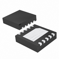
MAX16016PTBS+T Maxim Integrated Products, MAX16016PTBS+T Datasheet - Page 14

MAX16016PTBS+T
Manufacturer Part Number
MAX16016PTBS+T
Description
IC UP SUPERVISOR LP 10TDFN-EP
Manufacturer
Maxim Integrated Products
Type
Battery Backup Circuitr
Datasheet
1.MAX16021LTES.pdf
(21 pages)
Specifications of MAX16016PTBS+T
Number Of Voltages Monitored
1
Output
Open Drain or Open Collector
Reset
Active Low
Reset Timeout
145 ms Minimum
Voltage - Threshold
2.93V
Operating Temperature
-40°C ~ 85°C
Mounting Type
Surface Mount
Package / Case
10-TDFN Exposed Pad
Mounting Style
SMD/SMT
Lead Free Status / RoHS Status
Lead free / RoHS Compliant
Low-Power µP Supervisory Circuits with
Battery-Backup Circuit and Chip-Enable Gating
The Typical Application Circuit shows a typical connec-
tion using the MAX16020. OUT powers the static ran-
dom-access memory (SRAM). If V
reset threshold (V
higher than V
than V
OUT (see the Functional Diagrams ). In battery-backup
mode, an internal MOSFET connects the backup battery
to OUT. The on-resistance of the MOSFET is a function of
backup-battery voltage and temperature.
In a brownout or power failure, it may be necessary to
preserve the contents of the RAM. With a backup battery
installed at BATT, the MAX16016/MAX16020/MAX16021
automatically switch the RAM to the backup power when
V
BATTON output that goes high when in battery-backup
mode. These devices require two conditions before
switching to battery-backup mode:
1) V
2) V
Table 3 lists the status of the inputs and outputs in bat-
tery-backup mode. The device does not power up if the
only voltage source is on BATT. OUT only powers up
from V
The MAX16020/MAX16021 provide internal gating of
CE signals to prevent erroneous data from being written
to CMOS RAM in the event of a power failure or
Table 3. Input and Output Status in
Battery-Backup Mode
14
CC
BATTON, WDO
RESET/RESET
BATTOK, LL
CC
CC
______________________________________________________________________________________
falls. The MAX16016/MAX16020/MAX16021 have a
CEOUT
BATT
CEIN
TH
CC
OUT
V
PFO
PIN
must be below the reset threshold.
must be below V
CC
and V
at startup.
BATT
CC
Disconnected from OUT
Connected to BATT
Connected to OUT. Current drawn from the
battery is less than 0.55µA (at V
excluding I
Asserted
High state (push-pull), high impedance
(open-drain)
Low state
Disconnected from CEOUT
Pulled up to V
Not affected
, V
TH
is less than V
Backup-Battery Switchover
CC
), or if V
Detailed Description
connects to OUT. If V
BATT
OUT
.
CC
OUT
) when V
BATT
STATUS
is lower than V
CC
CE Signal Gating
, BATT connects to
is greater than the
CC
= 0V.
CC
BATT
is lower
TH
= 3V,
, but
brownout. During normal operation, the CE gate is
enabled and passes all CE transitions. When the reset
output asserts, this path becomes disabled, preventing
erroneous data from corrupting the CMOS RAM.
CEOUT is pulled up to OUT through an internal current
source. The 1.5ns propagation delay from CEIN to
CEOUT allows the devices to be used with most µPs
and high-speed DSPs.
During normal operation (reset not asserted), CEIN is
connected to CEOUT through a low on-resistance
transmission gate. If CEIN is high when a reset asserts,
CEOUT remains high regardless of any subsequent
transition on CEIN during the reset event.
If CEIN is low when reset asserts, CEOUT is held low
for 12µs to allow completion of the read/write operation.
After the 12µs delay expires, CEOUT goes high and
stays high regardless of any subsequent transitions on
CEIN during the reset event. When CEOUT is disconnect-
ed from CEIN, CEOUT is actively pulled up to OUT.
The propagation delay through the CE circuitry
depends on both the source impedance of the drive to
CEIN and the capacitive loading at CEOUT. Minimize
the capacitive load at CEOUT to minimize the propaga-
tion delay, and use a low output-impedance driver.
The low-line comparator monitors V
voltage typically 2.5% higher than the reset threshold
(see Table 2). LL asserts prior to a reset condition during
a brownout condition. On power-up, LL deasserts after
the reset output. LL can be used to provide a nonmask-
able interrupt (NMI) to the µP when the voltage begins to
fall to initiate an orderly software shutdown routine.
Many µP-based products require manual reset capability,
allowing the operator, a test technician, or external logic
circuitry to initiate a reset. For the MAX16016/MAX16020/
MAX16021, a logic-low on MR asserts RESET/RESET.
RESET/RESET remains asserted while MR is low. When
MR goes high RESET/RESET deasserts after a minimum
of 145ms (t
V
with open-drain/collector outputs. Connect a normally
open momentary switch from MR to GND to create a
manual reset function; external debounce circuitry is not
required. If MR is driven from a long cable or the device is
used in a noisy environment, connect a 0.1µF capacitor
from MR to GND to provide additional noise immunity.
CC
. MR can be driven with TTL/CMOS logic levels or
RP
). MR has an internal 30kΩ pullup resistor to
Low-Line Output ( LL )
Manual Reset Input
CC
with a threshold


