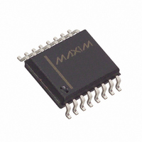
MAX696EWE+T Maxim Integrated Products, MAX696EWE+T Datasheet - Page 10

MAX696EWE+T
Manufacturer Part Number
MAX696EWE+T
Description
IC SUPERVISOR MPU 16-SOIC
Manufacturer
Maxim Integrated Products
Type
Battery Backup Circuitr
Datasheet
1.MAX696EWE.pdf
(15 pages)
Specifications of MAX696EWE+T
Number Of Voltages Monitored
2
Output
Push-Pull, Push-Pull
Reset
Active High/Active Low
Reset Timeout
35 ms Minimum
Voltage - Threshold
Adjustable/Selectable
Operating Temperature
-40°C ~ 85°C
Mounting Type
Surface Mount
Package / Case
16-SOIC (0.300", 7.5mm Width)
Lead Free Status / RoHS Status
Lead free / RoHS Compliant
The MAX697 uses two pins to control the CE or WRITE
inputs of CMOS RAMs. When LL
a buffered replica of CE IN, with a 50ns propagation
delay. If LL
max), an internal gate forces CE OUT high, indepen-
dent of CE IN. The CE output is also forced high when
V
CE OUT typically drives the CE, CS, or WRITE input of
battery backed up CMOS RAM. This ensures the
integrity of the data in memory by preventing write
operations when V
tection of EEPROMs can be achieved by using the CE
OUT to drive the STORE or WRITE inputs of an EEP-
ROM, EAROM, or NOVRAM.
If the 50ns typical propagation delay of CE OUT is too
long, connect CE IN to GND and use the resulting CE
OUT to control a high-speed external logic gate. A sec-
ond alternative is to AND the LOW LINE output with the
CE or WR signal. An external logic gate and the RESET
output of the MAX696/MAX697 can also be used for
CMOS RAM write protection.
Microprocessor Supervisory Circuits
Figure 5. MAX697 Reset Timing
10
CC
is less than V
______________________________________________________________________________________
IN
input falls below 1.3V (1.2V min, 1.4V
BATT
CC
RAM Write Protection
is at an invalid level. Similar pro-
. (See Figure 4.)
(MAX697) CE OUT
(MAX697) CE IN
LOW LINE
OUTPUT
OUTPUT
RESET
LL
CE Gating and
IN
IN
is > 1.3V, CE OUT is
50ms
1.3V
1.312V
The power-fail input (PFI) is compared to an internal
1.3V reference. The power-fail output (PFO) goes low
when the voltage at PFI is less than 1.3V. Typically PFI
is driven bay an external voltage-divider that senses
either the unregulated DC input to the system’s V
regulator or the regulated output. The voltage-divider
ration can be chosen so the voltage at PFI falls below
1.3V several milliseconds before the LL
1.3V. PFO is normally used to interrupt the micro-
processor so that data can be stored in RAM before
LL
The power-fail detector can also monitor the backup
battery to warn of a low-battery condition. To conserve
battery power, the power-fail detector comparator is
turned off and PFO is forced low when V
than the V
The watchdog circuit monitors the activity of the micro-
processor. If the microprocessor does not toggle the
watchdog input (WDI) within the selected timeout period,
a 50ms RESET pulse is generated. Since many systems
cannot service the watchdog timer immediately after a
reset, the MAX696/MAX697 have a longer timeout period
after a reset is issued. The normal timeout period
1.25V Comparator and Power-Fail Warning
IN
50ms
falls below 1.3V and the RESET output goes low.
1.3V
BATT
input voltage.
Watchdog Timer and Oscillator
1.312V
IN
CC
falls below
is lower
CC


