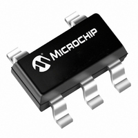
TC1015-3.0VCT713 Microchip Technology, TC1015-3.0VCT713 Datasheet - Page 6

TC1015-3.0VCT713
Manufacturer Part Number
TC1015-3.0VCT713
Description
IC REG LDO 3.0V 100MA SOT23A-5
Manufacturer
Microchip Technology
Specifications of TC1015-3.0VCT713
Package / Case
SOT-23-5, SC-74A, SOT-25
Regulator Topology
Positive Fixed
Voltage - Output
3V
Voltage - Input
Up to 6V
Voltage - Dropout (typical)
0.18V @ 100mA
Number Of Regulators
1
Current - Output
100mA (Min)
Operating Temperature
-40°C ~ 125°C
Mounting Type
Surface Mount
Number Of Outputs
1
Polarity
Positive
Input Voltage Max
6 V
Output Voltage
3 V
Output Type
Fixed
Dropout Voltage (max)
250 / 400 mV
Output Current
100 mA
Line Regulation
0.05 %
Load Regulation
0.5 %
Voltage Regulation Accuracy
2.5 %
Maximum Operating Temperature
+ 125 C
Mounting Style
SMD/SMT
Minimum Operating Temperature
- 40 C
Primary Input Voltage
4V
Output Voltage Fixed
3V
Dropout Voltage Vdo
180mV
No. Of Pins
5
Voltage Regulator Case Style
SOT-23
Operating Temperature Range
-40°C To +125°C
Rohs Compliant
Yes
Lead Free Status / RoHS Status
Lead free / RoHS Compliant
Current - Limit (min)
-
Lead Free Status / Rohs Status
Lead free / RoHS Compliant
Other names
158-2007-2
158-2007-2
TC10153.0VCT713TR
158-2007-2
TC10153.0VCT713TR
Available stocks
Company
Part Number
Manufacturer
Quantity
Price
Part Number:
TC1015-3.0VCT713
Manufacturer:
MICROCHIP/微芯
Quantity:
20 000
TC1014/TC1015/TC1185
3.0
The TC1014/TC1015/TC1185 are precision fixed
output voltage regulators. (If an adjustable version is
desired, please see the TC1070/TC1071/TC1187 data
sheet.) Unlike bipolar regulators, the TC1014/TC1015/
TC1185 supply current does not increase with load
current. In addition, V
regulation over the entire 0mA to I
load current ranges (an important consideration in RTC
and CMOS RAM battery back-up applications).
Figure 3-1 shows a typical application circuit. The
regulator is enabled any time the shutdown input
(SHDN) is at or above V
when SHDN is at or below V
controlled by a CMOS logic gate, or I/O port of a
microcontroller. If the SHDN input is not required, it
should be connected directly to the input supply. While
in shutdown, supply current decreases to 0.05µA
(typical), V
FIGURE 3-1:
DS21335B-page 6
(to CMOS Logic or Tie
Battery
+
Shutdown Control
to V
DETAILED DESCRIPTION
IN
OUT
+
1µF
if unused)
falls to zero volts.
GND
V
SHDN
IN
TC1014
TC1015
TC1185
OUT
TYPICAL APPLICATION
CIRCUIT
IH
remains stable and within
, and shutdown (disabled)
Bypass
V
OUT
IL
. SHDN may be
OUT
MAX
470pF
Reference
Bypass Cap
(Optional)
+
1µF
operating
V
OUT
3.1
A 470pF capacitor connected from the Bypass input to
ground reduces noise present on the internal
reference, which in turn significantly reduces output
noise. If output noise is not a concern, this input may be
left unconnected. Larger capacitor values may be
used, but results in a longer time period to rated output
voltage when power is initially applied.
3.2
A 1µF (min) capacitor from V
The output capacitor should have an effective series
resistance greater than 0.1Ω and less than 5Ω. A 1µF
capacitor should be connected from V
is more than 10 inches of wire between the regulator
and the AC filter capacitor, or if a battery is used as the
power source. Aluminum electrolytic or tantalum
capacitor types can be used. (Since many aluminum
electrolytic capacitors freeze at approximately -30°C,
solid tantalums are recommended for applications
operating below -25°C.) When operating from sources
other than batteries, supply-noise rejection and
transient response can be improved by increasing the
value of the input and output capacitors and employing
passive filtering techniques.
Bypass Input
Output Capacitor
©
2002 Microchip Technology Inc.
OUT
to ground is required.
IN
to GND if there


