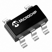
TC1016-3.3VCTTR Microchip Technology, TC1016-3.3VCTTR Datasheet - Page 8

TC1016-3.3VCTTR
Manufacturer Part Number
TC1016-3.3VCTTR
Description
IC CMOS LDO 80MA 3.3V SOT23-5
Manufacturer
Microchip Technology
Datasheets
1.TC101617EV.pdf
(22 pages)
2.TC1016-3.0VLTTR.pdf
(2 pages)
3.TC1016-3.3VCTTR.pdf
(20 pages)
Specifications of TC1016-3.3VCTTR
Package / Case
SOT-23-5, SC-74A, SOT-25
Regulator Topology
Positive Fixed
Voltage - Output
3.3V
Voltage - Input
Up to 6V
Voltage - Dropout (typical)
0.15V @ 80mA
Number Of Regulators
1
Current - Output
80mA (Min)
Operating Temperature
-40°C ~ 125°C
Mounting Type
Surface Mount
Polarity
Negative, Positive
Number Of Outputs
1
Output Type
Fixed
Output Voltage
3.3 V
Output Current
80 mA
Line Regulation
0.01 V
Load Regulation
0.1 mA
Dropout Voltage (max)
300 mV
Input Voltage Max
6 V
Maximum Operating Temperature
+ 125 C
Minimum Operating Temperature
- 40 C
Mounting Style
SMD/SMT
Output Voltage Tolerance
2 %
Voltage Regulation Accuracy
0.5 %
Lead Free Status / RoHS Status
Lead free / RoHS Compliant
Current - Limit (min)
-
Lead Free Status / Rohs Status
Lead free / RoHS Compliant
Available stocks
Company
Part Number
Manufacturer
Quantity
Price
Company:
Part Number:
TC1016-3.3VCTTR
Manufacturer:
MICROCHIP
Quantity:
12 000
Part Number:
TC1016-3.3VCTTR
Manufacturer:
MICROCHIP/微芯
Quantity:
20 000
TC1016
3.0
The descriptions of the pins are listed in Table 3-1.
TABLE 3-1:
3.1
The regulator is fully enabled when a logic-high is
applied to SHDN. The regulator enters shutdown when
a logic-low is applied to this input. During shutdown, the
output voltage falls to zero and the supply current is
reduced to 0.05 µA (typ.)
3.2
For best performance, it is recommended that the
ground pin be tied to a ground plane.
3.3
Bypass the regulated voltage output to GND with a
minimum capacitance of 1 µF. A ceramic bypass
capacitor is recommended for best performance.
DS21666B-page 8
SC-70
5-Pin
1
2
3
4
5
PIN DESCRIPTIONS
Shutdown Control Input (SHDN)
Ground Terminal (GND)
Regulated Voltage Output (V
5-Pin SOT-23
Pin No.
3
4
2
5
1
PIN FUNCTION TABLE
SHDN
Name
V
GND
V
NC
OUT
IN
Shutdown control input
No connect
Ground terminal
Regulated voltage output
Unregulated supply input
OUT
)
3.4
The minimum V
to ensure that the output maintains regulation:
V
maximum V
Power dissipation may limit V
order to maintain a junction temperature below 125°C.
Refer to Section 5.0 “Thermal Considerations”, for
determining junction temperature.
It is recommended that V
ceramic capacitor.
IN
2.7V and V
Function
Unregulated Supply Input (V
IN
should be less than or equal to 6V.
IN
IN
has to meet two conditions in order
[(V
© 2005 Microchip Technology Inc.
R
IN
+ 2.5%) + V
be bypassed to GND with a
IN
to a lower potential in
DROPOUT
IN
)
]. The


