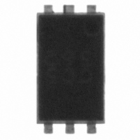
BH18MA3WHFV-TR Rohm Semiconductor, BH18MA3WHFV-TR Datasheet - Page 6

BH18MA3WHFV-TR
Manufacturer Part Number
BH18MA3WHFV-TR
Description
IC REG LDO 300MA 1.8V SD 6HVS0F
Manufacturer
Rohm Semiconductor
Series
-r
Specifications of BH18MA3WHFV-TR
Regulator Topology
Positive Fixed
Voltage - Output
1.8V
Voltage - Input
2.5 ~ 5.5 V
Number Of Regulators
1
Current - Output
300mA (Max)
Operating Temperature
-40°C ~ 85°C
Mounting Type
Surface Mount
Package / Case
6-HVSOF
Primary Input Voltage
5.5V
Output Voltage
1.8V
Dropout Voltage Vdo
60mV
No. Of Pins
6
Output Current
300mA
Voltage Regulator Case Style
HVSOF
Operating Temperature Range
-40°C To +85°C
Svhc
No
Number Of Outputs
1
Polarity
Positive
Input Voltage Max
5.5 V
Output Type
Fixed
Line Regulation
20 mV
Load Regulation
90 mV
Voltage Regulation Accuracy
1 %
Maximum Power Dissipation
0.68 W
Maximum Operating Temperature
+ 85 C
Mounting Style
SMD/SMT
Minimum Operating Temperature
- 40 C
Output Voltage Fixed
1.8V
Rohs Compliant
Yes
Featured Product
CMOS LDO Regulators
Voltage - Dropout (typical)
-
Current - Limit (min)
-
Lead Free Status / RoHS Status
Lead free / RoHS Compliant
Voltage - Dropout (typical)
-
Current - Limit (min)
-
Lead Free Status / Rohs Status
Lead free / RoHS Compliant
Available stocks
Company
Part Number
Manufacturer
Quantity
Price
Company:
Part Number:
BH18MA3WHFV-TR
Manufacturer:
ROHM
Quantity:
618
Part Number:
BH18MA3WHFV-TR
Manufacturer:
ROHM/罗姆
Quantity:
20 000
BH
• Over current protection circuit
• Actions in strong magnetic fields
• Thermal shutdown circuit
• Back current
• GND potential
www.rohm.com
© 2010 ROHM Co., Ltd. All rights reserved.
BH □□FB1WG series, BH□□FB1WHFV series,
BH □□LB1WG series, BH□□LB1WHFV series, BH □□MA3WHFV series
0.01
100
0.1
The IC incorporates a built-in over current protection circuit that operates according to the output current capacity. This circuit
serves to protect the IC from damage when the load is shorted. The protection circuits use fold-back type current limiting and
are designed to limit current flow by not latching up in the event of a large and instantaneous current flow originating from a
large capacitor or other component. These protection circuits are effective in preventing damage due to sudden and
unexpected accidents. However, the IC should not be used in applications characterized by the continuous operation or
transitioning of the protection circuits.
This system has a built-in thermal shutdown circuit for the purpose of protecting the IC from thermal damage. As shown
above, this must be used within the range of power dissipation, but if the power dissipation happens to be continuously
exceeded, the chip temperature increases, causing the thermal shutdown circuit to operate. When the thermal shutdown
circuit operates, the operation of the circuit is suspended. The circuit resumes operation immediately after the chip
temperature decreases, so the output repeats the ON and OFF states. There are cases in which the IC is destroyed due to
thermal runaway when it is left in the overloaded state. Be sure to avoid leaving the IC in the overloaded state.
Use caution when using the IC in the presence of a strong magnetic field as such environments may occasionally cause the chip
to malfunction.
In applications where the IC may be exposed to back current flow, it is recommended to create a route t dissipate this current
by inserting a bypass diode between the V
Ensure a minimum GND pin potential in all operating conditions.
In addition, ensure that no pins other than the GND pin carry a voltage less than or equal to the GND pin, including during
actual transient phenomena.
Input capacitor
Other precautions
Output capacitor
Examples of ceramic capacitor characteristics
10
To prevent oscillation at the output, it is recommended that the IC be operated at the stable region show in below Fig. It
operates at the capacitance of more than 1.0μF. As capacitance is larger, stability becomes more stable and characteristic of
output load fluctuation is also improved.
It is recommended to insert bypass capacitors between input and GND pins, positioning them as close to the pins as
possible. These capacitors will be used when the power supply impedance increases or when long wiring routes are used, so
they should be checked once the IC has been mounted.
Ceramic capacitors generally have temperature and DC bias characteristics. When selecting ceramic capacitors, use X5R or
X7R or better models that offer good temperature and DC bias characteristics and high torelant voltages.
1
0
Fig. 32 BH
Stable operating region characteristics (Example)
Cout=1.0μF
Fig. 29: Capacitance-bias characteristics (Y5V)
120
100
LB1WHFV/WG
80
60
40
20
0
0
10V torelance
Output current I
50
Stable region
LB1WHFV/WG
1
DC bias Vdc (V)
Ta= + 25°C
16V torelance
2
OUT
100
50V torelance
(mA)
3
150
4
BH
0.01
100
0.1
IN
10
1
Fig. 30: Capacitance-bias characteristics (X5R, X7R)
and V
0
Fig. 33 BH
Stable operating region characteristics (Example)
Cout=2.2μF
100
95
90
85
80
75
70
FB1WHFV/WG
0
OUT
Output current I
10V torelance
50
pins.
Stable region
FB1WHFV/WG
1
DC bias Vdc (V)
Ta= + 25°C
6/8
16V torelance
50V torelance
2
OUT
100
(mA)
3
150
4
BH
0.01
100
0.1
10
Fig. 34 BH
Stable operating region characteristics (Example)
1
0
Fig. 31: Capacitance–temperature characteristics
120
100
Cout=1.0μF
80
60
40
20
0
-25
MA3WHFV
(X5R, X7R, Y5V)
Output current I
100
MA3WHFV
0
Temperature (°C)
Stable region
Y5V
Cin=1.0μF
25
Technical Note
2010.07 - Rev. C
OUT
200
X7R
X5R
(mA)
50
Ta= + 25°C
75
300


