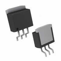
LM1085IS-12/NOPB National Semiconductor, LM1085IS-12/NOPB Datasheet - Page 9

LM1085IS-12/NOPB
Manufacturer Part Number
LM1085IS-12/NOPB
Description
IC REG LDO POS 12V 3A TO-263-3
Manufacturer
National Semiconductor
Datasheet
1.LM1085IT-ADJNOPB.pdf
(13 pages)
Specifications of LM1085IS-12/NOPB
Regulator Topology
Positive Fixed
Voltage - Output
12V
Voltage - Dropout (typical)
1.3V @ 3A
Number Of Regulators
1
Current - Output
3A
Current - Limit (min)
3.2A
Operating Temperature
-40°C ~ 125°C
Mounting Type
Surface Mount
Package / Case
TO-263-3, D²Pak (3 leads + Tab), TO-263AA
Primary Input Voltage
25V
Dropout Voltage Vdo
1.3V
No. Of Pins
3
Output Current
3A
Operating Temperature Range
-40°C To +125°C
Msl
MSL 3 - 168 Hours
Filter Terminals
SMD
Rohs Compliant
Yes
Input Voltage Primary Max
25V
Output Voltage Fixed
12V
Lead Free Status / RoHS Status
Lead free / RoHS Compliant
Voltage - Input
-
Other names
*LM1085IS-12
*LM1085IS-12/NOPB
LM1085IS-12
*LM1085IS-12/NOPB
LM1085IS-12
Application Note
must be added, one for case to heat-sink (θ
heatsink to ambient (θ
predicted as follows:
T
T
P
consumption is calculated as follows:
Once the devices power is determined, the maximum allow-
able (θ
θ
The LM1085 has different temperature specifications for two
different sections of the IC: the control section and the output
section. The Electrical Characteristics table shows the junc-
tion to case thermal resistances for each of these sections,
while the maximum junction temperatures (T
section is listed in the Absolute Maximum section of the
datasheet. T
T
θ
follows:
θ
θ
The required heat sink is determined by calculating its re-
quired thermal resistance (θ
JA(max)
JA(max)
JA
JA
J
J
J(max)
D
= T
is junction temperature, T
(max, OUTPUT SECTION) = (150˚C - T
is the power consumption of the device. Device power
(max, CONTROL SECTION) = (125˚C - T
A
JA(max)
is 150˚C for the output section.
+ P
= T
should be calculated separately for each section as
D
R(max)
J(max)
) is calculated as:
(θ
JC
/P
+ θ
is 125˚C for the control section, while
D
= T
CH
HA
). The junction temperature can be
+ θ
J(max
HA(max)
HA
A
(Continued)
− T
) = T
is ambient temperature, and
A(max)
).
A
FIGURE 7. Heat sink thermal Resistance vs Area
+ P
)/P
D
D
FIGURE 6. Power Dissipation Diagram
θ
A(max)
CH
JA
J(max)
A(max)
) and one for
)/P
) for each
)/P
D
D
9
Figure 6 shows the voltages and currents which are present
in the circuit.
θ
θ
θ
TROL SECTION) + θ
θ
SECTION) + θ
If thermal compound is used, θ
C/W. If the case is soldered to the heat sink, then a θ
be estimated as 0 C/W.
After, θ
lower of the two θ
heat sink.
If PC board copper is going to be used as a heat sink, then
Figure 7 can be used to determine the appropriate area
(size) of copper foil required.
HA(max)
HA(max)
HA(max)
HA(max)
I
P
IN
D
= I
HA(max)
= (V
=θ
= θ
should also be calculated twice as follows:
= θ
L
JA
10094764
+ I
JA(max)
IN
JA
(max, OUTPUT SECTION) - (θ
−V
G
CH
is calculated for each section, choose the
(max, CONTROL SECTION) - (θ
OUT
)
HA(max)
− (θ
10094716
) I
CH
L
JC
)
+ V
values to determine the appropriate
+ θ
IN
CH
I
G
CH
)
can be estimated at 0.2
JC
www.national.com
(OUTPUT
JC
CH
(CON-
can


