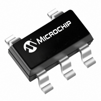
MCP1824T-ADJE/OT Microchip Technology, MCP1824T-ADJE/OT Datasheet - Page 19

MCP1824T-ADJE/OT
Manufacturer Part Number
MCP1824T-ADJE/OT
Description
IC LDO REG 300MA ADJ-V SOT23-5
Manufacturer
Microchip Technology
Datasheet
1.MCP1824T-1802EOT.pdf
(34 pages)
Specifications of MCP1824T-ADJE/OT
Regulator Topology
Positive Adjustable
Voltage - Output
0.8 ~ 5 V
Voltage - Input
2.1 ~ 6 V
Voltage - Dropout (typical)
0.2V @ 300mA
Number Of Regulators
1
Current - Output
300mA (Min)
Operating Temperature
-40°C ~ 125°C
Mounting Type
Surface Mount
Package / Case
SOT-23-5, SC-74A, SOT-25
Primary Input Voltage
6V
Output Voltage Adjustable Range
0.8V To 5V
Dropout Voltage Vdo
200mV
No. Of Pins
5
Output Current
300mA
Operating Temperature Range
-40°C To +125°C
Lead Free Status / RoHS Status
Lead free / RoHS Compliant
Current - Limit (min)
-
Lead Free Status / RoHS Status
Lead free / RoHS Compliant, Lead free / RoHS Compliant
Other names
MCP1824T-ADJE/OTTR
Available stocks
Company
Part Number
Manufacturer
Quantity
Price
Company:
Part Number:
MCP1824T-ADJE/OT
Manufacturer:
Microchip Technology
Quantity:
25 138
Part Number:
MCP1824T-ADJE/OT
Manufacturer:
MICROCHIP/微芯
Quantity:
20 000
4.3
The MCP1824/MCP1824S requires a minimum output
capacitance of 1 µF for output voltage stability. Ceramic
capacitors are recommended because of their size,
cost, and environmental robustness qualities.
Aluminum-electrolytic and tantalum capacitors can be
used on the LDO output as well. The Equivalent Series
Resistance (ESR) of the electrolytic output capacitor
must be no greater than 1 ohm. The output capacitor
should be located as close to the LDO output as is
practical. Ceramic materials X7R and X5R have low
temperature coefficients and are well within the
acceptable ESR range required. A typical 1 µF X7R
0805 capacitor has an ESR of 50 milli-ohms.
Larger LDO output capacitors can be used with the
MCP1824/MCP1824S
performance and power supply ripple rejection
performance. A maximum of 22 µF is recommended.
Aluminum-electrolytic capacitors are not recom-
mended for low temperature applications of < -25°C.
4.4
Low input source impedance is necessary for the LDO
output to operate properly. When operating from
batteries, or in applications with long lead length
(> 10 inches) between the input source and the LDO,
some input capacitance is recommended. A minimum
of 1.0 µF to 4.7 µF is recommended for most
applications.
For
requirements, the input capacitance of the LDO is very
important. The input capacitance provides the LDO
with a good local low-impedance source to pull the
transient currents from, in order to respond quickly to
the output load step. For good step response
performance, the input capacitor should be of
equivalent (or higher) value than the output capacitor.
The capacitor should be placed as close to the input of
the LDO as is practical. Larger input capacitors will also
help reduce any high-frequency noise on the input and
output of the LDO and reduce the effects of any
inductance that exists between the input source
voltage and the input capacitance of the LDO.
4.5
The PWRGD output is used to indicate when the output
voltage of the LDO is within 92% (typical value, see
Section 1.0 “Electrical Characteristics” for Minimum
and Maximum specifications) of its nominal regulation
value.
As the output voltage of the LDO rises, the PWRGD
output will be held low until the output voltage has
exceeded the power good threshold plus the hysteresis
value. Once this threshold has been exceeded, the
power good time delay is started (shown as T
Electrical Characteristics table). The power good time
2007 Microchip Technology Inc.
applications
Output Capacitor
Input Capacitor
Power Good Output (PWRGD)
that
to
have
improve
output
step
PG
dynamic
in the
load
MCP1824/MCP1824S
delay is fixed at 110 µs (typical). After the time delay
period, the PWRGD output will go high, indicating that
the output voltage is stable and within regulation limits.
If the output voltage of the LDO falls below the power
good threshold, the power good output will transition
low. The power good circuitry has a 200 µs delay when
detecting a falling output voltage, which helps to
increase noise immunity of the power good output and
avoid false triggering of the power good output during
fast output transients. See
timing characteristics.
When the LDO is put into Shutdown mode using the
SHDN input, the power good output is pulled low
immediately, indicating that the output voltage will be
out of regulation. The timing diagram for the power
good output when using the shutdown input is shown in
Figure
The power good output is an open-drain output that can
be pulled up to any voltage that is equal to or less than
the LDO input voltage. This output is capable of sinking
1.2 mA minimum (V
FIGURE 4-2:
FIGURE 4-3:
Shutdown.
V
V
PWRGD
VPWRGD_TH
IN
SHDN
OUT
VOUT
30 µs
PWRGD
4-3.
T
OR
70 µs
TPG
PWRGD
Power Good Timing.
Power Good Timing from
VOH
< 0.4V maximum).
Figure 4-2
T
PG
DS22070A-page 19
for power good
TVDET_PWRGD
VOL


