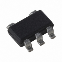
MIC5219-3.0YM5 TR Micrel Inc, MIC5219-3.0YM5 TR Datasheet - Page 9

MIC5219-3.0YM5 TR
Manufacturer Part Number
MIC5219-3.0YM5 TR
Description
IC REG LDO 500MA 1% 3.0V SOT23-5
Manufacturer
Micrel Inc
Datasheet
1.MIC5219-3.3YM5_TR.pdf
(14 pages)
Specifications of MIC5219-3.0YM5 TR
Regulator Topology
Positive Fixed
Voltage - Output
3V
Voltage - Input
Up to 12V
Voltage - Dropout (typical)
0.35V @ 500mA
Number Of Regulators
1
Current - Output
500mA
Operating Temperature
-40°C ~ 125°C
Mounting Type
Surface Mount
Package / Case
SOT-23-5, SC-74A, SOT-25
Lead Free Status / RoHS Status
Lead free / RoHS Compliant
Current - Limit (min)
-
Other names
576-2765-2
MIC5219-3.0YM5 TR
MIC5219-3.0YM5TR
MIC5219-3.0YM5TR
MIC5219-3.0YM5 TR
MIC5219-3.0YM5TR
MIC5219-3.0YM5TR
Applications Information
The MIC5219 is designed for 150mA to 200mA output current
applications where a high current spike (500mA) is needed for
short, start-up conditions. Basic application of the device will
be discussed initially followed by a more detailed discussion
of higher current applications.
Enable/Shutdown
Forcing EN (enable/shutdown) high (>2V) enables the
regulator. EN is compatible with CMOS logic. If the enable/
shutdown feature is not required, connect EN to IN (supply
input). See Figure 5.
Input Capacitor
A 1µF capacitor should be placed from IN to GND if there is
more than 10 inches of wire between the input and the AC
filter capacitor or if a battery is used as the input.
Output Capacitor
An output capacitor is required between OUT and GND to
prevent oscillation. The minimum size of the output capacitor
is dependent upon whether a reference bypass capacitor is
used. 1µF minimum is recommended when C
(see Figure 5). 2.2µF minimum is recommended when C
is 470pF (see Figure 6). For applications < 3V, the output
capacitor should be increased to 22µF minimum to reduce
start-up overshoot. Larger values improve the regulator’s
transient response. The output capacitor value may be in-
creased without limit.
The output capacitor should have an ESR (equivalent series
resistance) of about 1Ω or less and a resonant frequency
above 1MHz. Ultra-low-ESR capacitors could cause oscilla-
tion and/or underdamped transient response. Most tantalum
or aluminum electrolytic capacitors are adequate; film types
will work, but are more expensive. Many aluminum electro-
lytics have electrolytes that freeze at about –30°C, so solid
tantalums are recommended for operation below –25°C.
At lower values of output current, less output capacitance is
needed for stability. The capacitor can be reduced to 0.47µF
for current below 10mA, or 0.33µF for currents below 1mA.
No-Load Stability
The MIC5219 will remain stable and in regulation with no load
(other than the internal voltage divider) unlike many other
voltage regulators. This is especially important in CMOS
RAM keep-alive applications.
Reference Bypass Capacitor
BYP is connected to the internal voltage reference. A 470pF
capacitor (C
reference, providing a significant reduction in output noise
(ultra-low-noise performance). C
phase margin; when using C
or greater are generally required to maintain stability.
The start-up speed of the MIC5219 is inversely proportional
to the size of the reference bypass capacitor. Applications
requiring a slow ramp-up of output voltage should consider
larger values of C
consider omitting C
June 2009
BYP
) connected from BYP to GND quiets this
BYP
BYP
. Likewise, if rapid turn-on is necessary,
.
BYP
, output capacitors of 2.2µF
BYP
reduces the regulator
BYP
is not used
BYP
9
Thermal Considerations
The MIC5219 is designed to provide 200mA of continuous
current in two very small profile packages. Maximum power
dissipation can be calculated based on the output current and
the voltage drop across the part. To determine the maximum
power dissipation of the package, use the thermal resistance,
junction-to-ambient, of the device and the following basic
equation.
T
125°C, and T
is layout dependent; Table 1 shows examples of thermal
resistance, junction-to-ambient, for the MIC5219.
2×2 Thin
MLF
The actual power dissipation of the regulator circuit can be
determined using one simple equation.
Substituting P
conditions that are critical to the application will give the
maximum operating conditions for the regulator circuit. For
example, if we are operating the MIC5219-3.3BM5 at room
temperature, with a minimum footprint layout, we can deter-
mine the maximum input voltage for a set output current.
The thermal resistance, junction-to-ambient, for the minimum
footprint is 220°C/W, taken from Table 1. The maximum power
dissipation number cannot be exceeded for proper opera-
tion of the device. Using the output voltage of 3.3V, and an
output current of 150mA, we can determine the maximum
input voltage. Ground current, maximum of 3mA for 150mA
of output current, can be taken from the “Electrical Charac-
teristics” section of the data sheet.
Therefore, a 3.3V application at 150mA of output current
can accept a maximum input voltage of 6.2V in a SOT-23-5
package. For a full discussion of heat sinking and thermal
effects on voltage regulators, refer to the “Regulator Ther-
mals” section of Micrel’s Designing with Low-Dropout Voltage
Regulators handbook.
Package
MM8
SOT-23-5 (M5)
2×2 MLF
J
(max) is the maximum junction temperature of the die,
®
®
P
P
P
P
455mW = (V
455mW = (150mA) × V
950mW = 153mA × V
V
(MT)
(MM)
D
D
D
IN
D
(max ) =
(max) = 455mW
(max ) =
®
= (V
Table 1. MIC5219 Thermal Resistance
= 6.2V
(ML)
IN
A
D
is the ambient operating temperature. θ
(max) for P
– V
θ
Minimum Footprint
MAX
(
JA
T
IN
(
OUT
125 °C − 25°C
J
Recommended
(max ) − T
– 3.3V) × 150mA + V
160°C/W
220°C/W
220°C / W
90°C/W
90°C/W
θ
) I
JA
OUT
D
IN
IN
+ V
and solving for the operating
A
+ 3mA × V
)
IN
I
)
GND
θ
2oz. Copper
JA
170°C/W
70°C/W
1" Square
IN
IN
—
—
× 3mA
– 495mW
M0371-061809
130°C/W
30°C/W
θ
—
—
JC
JA


