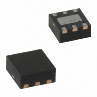
MIC5319-1.8YML TR Micrel Inc, MIC5319-1.8YML TR Datasheet - Page 4

MIC5319-1.8YML TR
Manufacturer Part Number
MIC5319-1.8YML TR
Description
IC REG LDO 500MA 1.8V 6-MLF
Manufacturer
Micrel Inc
Datasheet
1.MIC5319YML_TR.pdf
(12 pages)
Specifications of MIC5319-1.8YML TR
Regulator Topology
Positive Fixed
Voltage - Output
1.8V
Voltage - Input
2.5 ~ 5.5 V
Number Of Regulators
1
Current - Output
500mA
Current - Limit (min)
600mA
Operating Temperature
-40°C ~ 125°C
Mounting Type
Surface Mount
Package / Case
6-MLF®, QFN
Lead Free Status / RoHS Status
Lead free / RoHS Compliant
Voltage - Dropout (typical)
-
Other names
576-1903-2
MIC5319-1.8YMLTR
MIC5319-1.8YMLTR
MIC5319-1.8YMLTR
MIC5319-1.8YMLTR
Absolute Maximum Ratings
Supply Input Voltage (V
Enable Input Voltage (V
Power Dissipation (P
Junction Temperature (T
Storage Temperature (T
Lead Temperature (soldering, 5sec.)......................... 260°C
ESD Rating
Electrical Characteristics
V
Parameter
Output Voltage Accuracy
Feedback Voltage
(ADJ Option)
Line Regulation
Load Regulation
Dropout Voltage
Ground Pin Current
Ground Pin Current in
Shutdown
Ripple Rejection
Current Limit
Output Voltage Noise
Turn-On Time
Enable Input Voltage
Enable Input Current
Notes:
1.
2.
3.
4.
5.
6.
7.
8.
9.
Micrel, Inc.
May 2010
IN
= V
Exceeding the absolute maximum rating may damage the device.
The device is not guaranteed to function outside its operating rating.
The maximum allowable power dissipation of any T
power dissipation will result in excessive die temperature, and the regulator may go into thermal shutdown.
Devices are ESD sensitive. Handling precautions recommended. Human body model.
Specification for packaged product only.
Regulation is measured at constant junction temperature using low duty cycle pulse testing.
Dropout voltage is defined as the input-to-output differential at which the output voltage drops 2% below its nominal V
dropout voltage spec does not apply, as part is limited by minimum V
For ADJ option, V
Ground pin current is the regulator quiescent current. The total current drawn from the supply is the sum of the load current plus the ground pin
current.
OUT
+1.0V; C
(4)
.................................................................. 3kV
(7, 8)
(6)
(9)
OUT
OUT
D
= 2.2µF; I
= 3V for dropout specification.
) ........................... Internally Limited
IN
EN
S
J
)...................................... 0V to 6V
)......................... −65°C to +150°C
Condition
Variation from nominal V
Variation from nominal V
V
I
I
I
I
V
f = up to 1kHz; C
f = 10kHz; C
V
C
C
Logic Low (Regulator Shutdown)
Logic High (Regulator Enabled)
V
V
) ........................ −40°C to +125°C
OUT
OUT
OUT
OUT
)..................................... 0V to 6V
IN
EN
OUT
IL
IH
OUT
OUT
= ≤ 0.2V (Regulator Shutdown)
= V
= ≥ 1.0V (Regulator Shutdown)
≤ 0.2V
= 100µA to 500mA
= 50mA
= 500mA
= 0 to 500mA
OUT
= 0V
= 2.2µF; C
= 2.2µF; C
OUT
= 100µA; T
(4)
+1V to 5.5V
OUT
(1)
BYP
BYP
= 2.2µF ceramic; C
OUT
= 0.1 µF; 10Hz to 100kHz
= 0.1 µF
J
= 2.2µF ceramic; C
= 25°C, bold values indicate –40°C to +125°C, unless noted.
A
(ambient temperature) is P
OUT
OUT
, I
OUT
= 100mA to 500mA
BYP
(3)
IN
= 0.1 µF
spec of 2.5V. There may be some typical dropout degradation at V
BYP
4
Operating Ratings
Supply Input Voltage (V
Enable Input Voltage (V
Junction Temperature (T
Package Thermal Resistance
= 0.1 µF
MLF
TSOT-23 (θ
D
(max) = (T
®
(θ
JA
)..........................................................93°C/W
J(max)
1.2375
JA
1.225
Min.
−1.0
−2.0
600
1.2
) ..................................................235°C/W
− T
A
) / θ
IN
EN
JA
J
)............................ +2.5V to +5.5V
(2)
) ........................ −40°C to +125°C
)..................................... 0V to V
. Exceeding the maximum allowable
Typ.
1.25
1.25
0.04
0.01
0.01
200
700
0.1
0.5
20
90
70
60
40
40
OUT
. For outputs below 2.5V,
1.2625
1.275
Max.
+1.0
+2.0
400
150
100
0.3
0.5
0.2
40
1
1
M9999-052510
MIC5319
µVrms
OUT
Units
%/V
mV
mA
µA
µA
dB
µA
µs
%
%
V
V
<3V.
IN


