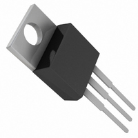
LT1086CT-3.6 Linear Technology, LT1086CT-3.6 Datasheet - Page 9

LT1086CT-3.6
Manufacturer Part Number
LT1086CT-3.6
Description
IC LDO REG 1.5A 3.6V TO-220-3
Manufacturer
Linear Technology
Datasheet
1.LT1086CTPBF.pdf
(16 pages)
Specifications of LT1086CT-3.6
Regulator Topology
Positive Fixed
Voltage - Output
3.6V
Voltage - Input
Up to 20V
Voltage - Dropout (typical)
1.3V @ 1.5A
Number Of Regulators
1
Current - Limit (min)
1.5A
Operating Temperature
0°C ~ 150°C
Mounting Type
Through Hole
Package / Case
TO-220-3 (Straight Leads)
Lead Free Status / RoHS Status
Contains lead / RoHS non-compliant
Current - Output
-
Available stocks
Company
Part Number
Manufacturer
Quantity
Price
Company:
Part Number:
LT1086CT-3.6
Manufacturer:
LT
Quantity:
3
Part Number:
LT1086CT-3.6#PBF
Manufacturer:
LINEAR/凌特
Quantity:
20 000
APPLICATIONS
plugging and unplugging in the system will not generate
current large enough to do any damage.
The adjustment pin can be driven on a transient basis
degradation. Of course as with any IC regulator, exceeding
the maximum input-to-output voltage differential causes
the internal transistors to break down and none of the
protection circuitry is functional.
Overload Recovery
Like any of the IC power regulators, the LT1086 has safe
area protection. The safe area protection decreases the
current limit as input-to-output voltage increases and
keeps the power transistor inside a safe operating region
for all values of input-to-output voltage. The LT1086
protection is designed to provide some output current at
all values of input-to-output voltage up to the device
breakdown.
When power is first turned on, as the input voltage rises,
the output follows the input, allowing the regulator to start
up into very heavy loads. During the start-up, as the input
voltage is rising, the input-to-output voltage differential
remains small, allowing the regulator to supply large
output currents. With high input voltage, a problem can
occur wherein removal of an output short will not allow the
output voltage to recover. Older regulators such as the
7800 series also exhibited this phenomenon, so it is not
unique to the LT1086.
The problem occurs with a heavy output load when the
input voltage is high and the output voltage is low, such as
immediately after a removal of a short. The load line for
such a load may intersect the output current curve at two
points. If this happens there are two stable output operat-
ing points for the regulator. With this double intersection
25V, with respect to the output without any device
V
IN
IN
(OPTIONAL)
U
1N4002
LT1086
+
ADJ
D1
INFORMATION
C
10 F
U
ADJ
OUT
W
R1
R2
+
C
150 F
LT1086 • AI01
OUT
V
U
OUT
the power supply may need to be cycled down to zero and
brought up again to make the output recover.
Ripple Rejection
For the LT1086 the typical curves for ripple rejection
reflect values for a bypassed adjust pin. This curve will be
true for all values of output voltage. For proper bypassing
and ripple rejection approaching the values shown, the
impedance of the adjust pin capacitor at the ripple fre-
quency should equal the value of R1, (normally 100 to
120 ). The size of the required adjust pin capacitor is a
function of the input ripple frequency. At 120Hz the adjust
pin capacitor should be 13 F if R1 = 100 ; at 10kHz only
0.16 F is needed.
For circuits without an adjust pin bypass capacitor the
ripple rejection will be a function of output voltage. The
output ripple will increase directly as a ratio of the output
voltage to the reference voltage (V
ample, with the output voltage equal to 5V and no adjust
pin capacitor, the output ripple will be higher by the ratio
of 5V/1.25V or four times larger. Ripple rejection will be
degraded by 12dB from the value shown on the LT1086
curve. Typical curves are provided for the 5V and 12V
devices since the adjust pin is not available.
Output Voltage
The LT1086 develops a 1.25V reference voltage between
the output and the adjust terminal (see Figure 1). By
placing resistor R1 between these two terminals, a con-
stant current is caused to flow through R1 and down
through R2 to set the overall output voltage. Normally this
current is chosen to be the specified minimum load
current of 10mA. Because I
when compared with the current through R1, it repre-
sents a small error and can usually be ignored. For fixed
voltage devices R1 and R2 are included in the device.
V
IN
V
OUT
IN
= V
Figure 1. Basic Adjustable Regulator
50 A
REF
I
ADJ
LT1086
1 +
ADJ
R2
R1
+ I
OUT
ADJ
ADJ
R2
V
REF
is very small and constant
LT1086 Series
R2
R1
OUT
+
/V
10 F
TANTALUM
REF
). For ex-
1086 • F01
sn1086 1086ffs
V
OUT
9


