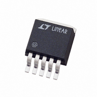
LT1129IQ-3.3 Linear Technology, LT1129IQ-3.3 Datasheet - Page 11

LT1129IQ-3.3
Manufacturer Part Number
LT1129IQ-3.3
Description
IC LDO REG W/SHTDWN 3.3V DDPAK-5
Manufacturer
Linear Technology
Datasheet
1.LT1129CTPBF.pdf
(16 pages)
Specifications of LT1129IQ-3.3
Regulator Topology
Positive Fixed
Voltage - Output
3.3V
Voltage - Input
4.15 ~ 30 V
Voltage - Dropout (typical)
0.45V @ 700mA
Number Of Regulators
1
Current - Output
700mA
Operating Temperature
-40°C ~ 125°C
Mounting Type
Surface Mount
Package / Case
TO-263-5, D²Pak (5 leads + Tab), TO-263BA
Lead Free Status / RoHS Status
Contains lead / RoHS non-compliant
Current - Limit (min)
-
Available stocks
Company
Part Number
Manufacturer
Quantity
Price
Company:
Part Number:
LT1129IQ-3.3
Manufacturer:
INMOS
Quantity:
23
Part Number:
LT1129IQ-3.3
Manufacturer:
LT
Quantity:
20 000
Company:
Part Number:
LT1129IQ-3.3#TRPBF
Manufacturer:
AD
Quantity:
21
OPERATION
copper. This data can be used as a rough guideline in
estimating thermal resistance. The thermal resistance for
each application will be affected by thermal interactions
with other components as well as board size and shape.
Some experimentation will be necessary to determine the
actual value.
Table 1. Q Package, 5-Lead DD
TOPSIDE*
2500 sq. mm 2500 sq. mm 2500 sq. mm
1000 sq. mm 2500 sq. mm 2500 sq. mm
125 sq. mm
* Tab of device attached to topside copper
Table 2. ST Package, 3-Lead SOT-223
TOPSIDE*
2500 sq. mm 2500 sq. mm 2500 sq. mm
1000 sq. mm 2500 sq. mm 2500 sq. mm
225 sq. mm
100 sq. mm
* Tab of device attached to topside copper
Table 3. S8 Package, 8-Lead Plastic SOIC
TOPSIDE*
2500 sq. mm 2500 sq. mm 2500 sq. mm
1000 sq. mm 2500 sq. mm 2500 sq. mm
225 sq. mm
100 sq. mm
* Device attached to topside copper
T Package, 5-Lead TO-220
Thermal Resistance (Junction-to-Case) = 5°C/W
Calculating Junction Temperature
Example: Given an output voltage of 3.3V, an input voltage
range of 4.5V to 5.5V, an output current range of 0mA to
500mA, and a maximum ambient temperature of 50°C,
what will the maximum junction temperature be?
COPPER AREA
COPPER AREA
COPPER AREA
2500 sq. mm 2500 sq. mm
2500 sq. mm 2500 sq. mm
2500 sq. mm 2500 sq. mm
2500 sq. mm 2500 sq. mm
2500 sq. mm 2500 sq. mm
BACKSIDE
BACKSIDE
BACKSIDE
BOARD AREA
BOARD AREA
BOARD AREA
(JUNCTION-TO-AMBIENT)
(JUNCTION-TO-AMBIENT)
(JUNCTION-TO-AMBIENT)
THERMAL RESISTANCE
THERMAL RESISTANCE
THERMAL RESISTANCE
25°C/W
45°C/W
55°C/W
27°C/W
35°C/W
45°C/W
53°C/W
59°C/W
55°C/W
63°C/W
69°C/W
The power dissipated by the device will be equal to:
where, I
so,
If we use a DD package, then the thermal resistance will be
in the range of 25°C/W to 35°C/W depending on copper
area. So the junction temperature rise above ambient will
be approximately equal to:
The maximum junction temperature will then be equal to
the maximum junction temperature rise above ambient
plus the maximum ambient temperature or:
Output Capacitance and Transient Performance
The LT1129 is designed to be stable with a wide range
of output capacitors. The minimum recommended value
is 3.3μF with an ESR of 2Ω or less. The LT1129 is a
micropower device and output transient response will
be a function of output capacitance. See the Transient
Response curves in the Typical Performance Character-
istics. Larger values of output capacitance will decrease
the peak deviations and provide improved output transient
response. Bypass capacitors, used to decouple individual
components powered by the LT1129, will increase the
effective value of the output capacitor.
Protection Features
The LT1129 incorporates several protection features
which make it ideal for use in battery-powered circuits.
In addition to the normal protection features associated
with monolithic regulators, such as current limiting and
thermal limiting, the device is protected against reverse
input voltages, and reverse voltages from output to input.
For fi xed voltage devices the output and sense pins are
tied together at the output.
LT1129/LT1129-3.3/LT1129-5
1.24W • 30°C/W = 37.2°C
T
JMAX
I
V
I
P = 500mA • (5.5V – 3.3V) + (25mA • 5.5V)
OUT MAX
OUT MAX
GND
= 50°C + 37.2°C = 87.2°C
IN MAX
= 1.24W
at (I
= 5.5V
• (V
OUT
= 500mA
IN MAX
= 500mA, V
– V
OUT
IN
) + (I
= 5.5V) = 25mA
GND
• V
IN MAX
11
112935ff
)


