P850-G200-WH Bourns Inc., P850-G200-WH Datasheet
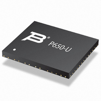
SURGE SUPP TBU 200MA 850VIMP SMD

P850-G200-WH

Manufacturer Part Number
P850-G200-WH
Description
SURGE SUPP TBU 200MA 850VIMP SMD
Manufacturer
Bourns Inc.
Series
TBU™r
Datasheets

Specifications of P850-G200-WH

Voltage - Working
425V
Technology
Mixed Technology
Number Of Circuits
2
Applications
SLIC
Package / Case
0.325" L x 0.157 " W x 0.033" H (8.25mm x 4mm x 0.85mm)
Voltage Rating
850 V
Current Rating
200 mA
Height
0.85 mm
Length
8.25 mm
Mounting
SMD/SMT
Operating Temperature Range
- 40 C to + 85 C
Termination Style
SMD/SMT
Width
4 mm
Suppressor Type
Data Line / Mains
Output Current
400mA
Peak Surge Current
200mA
Response Time
1µs
Resistance
55ohm
Operating Temperature Max
85°C
Clamping Voltage Vc Max
850V
Length/height, External
0.85mm
Rohs Compliant
Yes
External Depth
4mm
External Width
8.25mm
Lead Free Status / RoHS Status
Lead free / RoHS Compliant
Power (watts)
-
Voltage - Clamping
-
Lead Free Status / Rohs Status
Lead free / RoHS Compliant
Bourns
TBU
protection components designed to
protect Subscriber Line Interface Circuits
(SLICs) against transients caused by
AC power cross, induction and lightning
surges.
The TBU
provides an effective barrier behind
which sensitive electronics are not
exposed to large voltages or currents
during surge events.
*RoHS Directive 2002/95/EC Jan 27 2003 including Annex.
Specifi cations are subject to change without notice.
Customers should verify actual device performance in their specifi c applications
The P-G series TBU
Symbol
I
I
I
R
R
t
I
V
Symbol
V
V
T
T
op
trigger
out
quiescent
block
Transient Blocking Units - TBU
Electrical Characteristics (T
Absolute Maximum Ratings (T
reset
imp
rms
op
stg
TBU
bal
products are high speed, surge
®
Model P500-G and P850-G
device blocks surges and
Parameter
Maximum protection voltage for impulse faults with rise time
Maximum protection voltage for continuous V
Operating temperature range
Storage temperature range
Parameter
Maximum current through the device that will not cause
current blocking
Typical current for the device to go from normal operating
state to protected state
Maximum current through the device
Series resistance of the TBU
Line-to line series resistance difference between two TBU
Maximum time for the device to go from normal operating
state to protected state
Current through the triggered TBU
voltage
Voltage below which the triggered TBU
normal operating state
devices are bidirectional; specifi cations are valid in both directions.
amb
Devices
amb
= 25 °C)
= 25 °C)
device
Features
UL recognized component File # E315805.
TBU
Telcordia
ITU-T
device with 50 Vdc circuit
Agency Approval
Industry Standards
Formerly
Extremely high speed performance
Blocks high voltages and currents
Two TBU
Simple, superior circuit protection
Minimal PCB area
RoHS compliant*, UL Recognized
device will transition to
P500-G and P850-G Protectors
rms
protectors in one small package
faults
brand
GR-1089
K.20, K.20E, K.21, K.21E, K.45
devices
P500-G120-WH
P500-G200-WH
P850-G120-WH
P850-G200-WH
P500-G120-WH
P500-G200-WH
P850-G120-WH
P850-G200-WH
P500-G120-WH
P500-G200-WH
P850-G120-WH
P850-G200-WH
Description
1 µsec
P500-Gxxx-WH
P850-Gxxx-WH
P500-Gxxx-WH
P850-Gxxx-WH
Port Type 2, 4
Port Type 3, 5
Applications
Min.
POTS linecards
VolP equipment
Voice and data combo linecards
ONU, ONT
Gateways
Cable and DSL modems
-65 to +150
-40 to +85
Typ.
150
275
150
275
0.7
50
22
Value
500
850
300
425
Max.
100
200
100
200
200
400
200
400
55
2
1
P500-G
P850-G
P850-G
Model
Unit
°C
°C
V
V
Unit
mA
mA
mA
mA
µs
V

Related parts for P850-G200-WH

P850-G200-WH Summary of contents

Page 1

... K.20, K.20E, K.21, K.21E, K.45 1 µsec faults rms P500-G120-WH P500-G200-WH P850-G120-WH P850-G200-WH P500-G120-WH P500-G200-WH P850-G120-WH P850-G200-WH P500-G120-WH P500-G200-WH P850-G120-WH P850-G200-WH ™ device ™ devices ™ device with 50 Vdc circuit ™ device will transition to Applications POTS linecards ■ VolP equipment ■ ■ ...

Page 2

... TBU P500-G and P850-G Protectors Typical Performance Characteristics V-I Characteristics +I I trigger -V reset V reset -I trigger Trigger Current Temperature 140 120 100 -40 - Temperature (°C) Time to Block vs. Fault Current 1 0.1 0.01 0.001 0.0001 +V 0.00001 0.000001 0.0000001 Customers should verify actual device performance in their specifi c applications ...

Page 3

... Specifi cations are subject to change without notice. Customers should verify actual device performance in their specifi c applications ™ device. For each graph the fault voltage, protected side voltage, V1 Tip Pxxx-G Ring P850-G Lightning, 850 P850-G Power Fault, 230 Vrms Ch3 Current s/div. µ Ch1 V1 Ch2 V2 ...

Page 4

... PIN 1 D TOP VIEW SIDE VIEW Pads 1A and 1 are internally connected; the same for pads 3A with 3, 4A with 4, and 6A with 6. This allows for one PCB layout to accommodate the P500 or P850. Recommended Pad Layout P500-Gxxx 0.75 (.030) 1.225 1.15 1.275 (.048) (.045) ( ...

Page 5

... TBU ™ P500-G and P850-G Protectors Thermal Resistances Part # Symbol Parameter Junction to leads (package) P500-G R th(j-a) Junction to leads (per TBU Junction to leads (package) P850-G R th(j-a) Junction to leads (per TBU Refl ow Profi le Profi le Feature Average Ramp-Up Rate (Tsmax to Tp) Preheat - Temperature Min ...

Page 6

... MM DIMENSIONS: (INCHES) Customers should verify actual device performance in their specifi c applications MANUFACTURER’S MARKING NUMBER TRADEMARK* 50GA = P500-G120-WH 50GB = P500-G200-WH 85GA = P850-G120-WH 85GB = P850-G200-WH MANUFACTURING DATE CODE PIN 1 *TRANSITION FROM FULTEC TRADEMARK TO BOURNS TRADEMARK IN 2009 CENTER EMBOSSMENT LINES OF ...

Page 7

... CNR Centra Science Ceramate Technical Vishay Diodes Inc. P500-G Solution: 5000 V Lightning 2/10 µsec, 500 A Source Bourns, Inc. CNR Centra Science Ceramate Technical Vishay Diodes Inc. P850-G Solution: 4000 V Lightning 10/700 µsec, 100 A ® GDTs and a diode 500 ns/div. Ch1 V1 Ch2 V2 Ch3 Current 2 1 500 ns/div ...

Related keywords