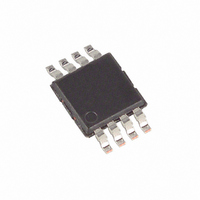
MAX1792EUA18+ Maxim Integrated Products, MAX1792EUA18+ Datasheet - Page 8

MAX1792EUA18+
Manufacturer Part Number
MAX1792EUA18+
Description
IC REG LDO 1.8V/ADJ 500MA 8-UMAX
Manufacturer
Maxim Integrated Products
Datasheet
1.MAX1792EUA15.pdf
(11 pages)
Specifications of MAX1792EUA18+
Regulator Topology
Positive Fixed or Adjustable
Voltage - Output
1.8V, 1.25 ~ 5 V
Voltage - Input
2.5 ~ 5.5 V
Number Of Regulators
1
Current - Output
500mA (Min)
Operating Temperature
-40°C ~ 85°C
Mounting Type
Surface Mount
Package / Case
8-MSOP, Micro8™, 8-uMAX, 8-uSOP,
Number Of Outputs
2
Polarity
Positive
Input Voltage Max
5.5 V
Output Voltage
1.25 V to 5 V, 1.8 V
Output Type
Adjustable, Fixed
Dropout Voltage (max)
360 mV
Output Current
500 mA
Line Regulation
0.15 %/V
Load Regulation
0.4 %
Voltage Regulation Accuracy
1.5 %
Maximum Power Dissipation
1.3 W
Maximum Operating Temperature
+ 85 C
Mounting Style
SMD/SMT
Minimum Operating Temperature
- 40 C
Reference Voltage
1.25 V
Lead Free Status / RoHS Status
Lead free / RoHS Compliant
Voltage - Dropout (typical)
-
Current - Limit (min)
-
Lead Free Status / Rohs Status
Lead free / RoHS Compliant
The MAX1792 does not suffer from these problems and
consumes only 110µA of quiescent current under
heavy loads as well as in dropout.
The MAX1792’s Dual Mode operation allows operation
in either a preset voltage mode or an adjustable mode.
Connect SET to GND to select the preset output volt-
age. The two-digit part number suffix identifies the out-
put voltage (see Selector Guide). For example, the
MAX1792EUA33 has a preset 3.3V output voltage.
The output voltage may also be adjusted by connecting
a voltage-divider from OUT to SET to GND (Figure 2).
Select R2 in the 25kΩ to 100kΩ range. Calculate R1
with the following equation:
where V
5.0V.
Pull SHDN low to enter shutdown. During shutdown, the
output is disconnected from the input and supply current
drops to 0.1µA. When in shutdown, RST pulls low and
OUT is discharged through an internal 5kΩ resistor. The
capacitance and load at OUT determine the rate at
which V
+6V, regardless of the input and output voltage.
500mA Low-Dropout
Linear Regulator in µMAX
Figure 2. Adjustable Output Using External Feedback
Resistors
8
V
IN
_______________________________________________________________________________________
= +2.5V TO +5.5V
ON
OFF
SET
OUT
1μF
C
IN
= 1.25V and V
decays. SHDN can be pulled as high as
R1 = R2 [(V
IN
IN
SHDN
RST
MAX1792
Output Voltage Selection
OUT
OUT
GND
OUT
OUT
/ V
SET
may range from 1.25V to
SET
) - 1]
C
3.3μF
OUT
R1 = R2
Shutdown
1.25V
R
V
R
2
OUT
1
V
- 1
OUT
The reset output (RST) pulls low when OUT is less than
93% of the nominal regulation voltage. Once OUT
exceeds 93% of the nominal voltage, RST goes high
impedance after 4ms. RST is an open-drain N-channel
output. To obtain a voltage output, connect a pullup
resistor from RST to OUT. A 100kΩ resistor works well for
most applications. RST can be used as a power-on-reset
(POR) signal to a microcontroller (µC), or drive an exter-
nal LED to indicate power failure. When the MAX1792 is
shut down, RST is held low independent of the output
voltage. If unused, leave RST grounded or unconnected.
The MAX1792 monitors and controls the pass transis-
tor’s gate voltage, limiting the output current to 0.8A
(typ). This current limit doubles when the output voltage
is within 4% of the nominal value to improve perfor-
mance with large load transients. The output can be
shorted to ground for an indefinite period of time with-
out damaging the part.
Thermal overload protection limits total power dissipa-
tion in the MAX1792. When the junction temperature
exceeds T
pass transistor, allowing the device to cool. The thermal
sensor turns the pass transistor on again after the junc-
tion temperature cools by 20°C, resulting in a pulsed
output during continuous thermal overload conditions.
Thermal overload protection protects the MAX1792 in
the event of fault conditions. For continuous operation,
do not exceed the absolute maximum junction-temper-
ature rating of T
The MAX1792’s maximum power dissipation depends on
the thermal resistance of the IC package and circuit
board, the temperature difference between the die junc-
tion and ambient air, and the rate of air flow. The power
dissipated in the device is P = I
maximum allowed power dissipation is 1.3W or:
where T
the MAX1792 die junction and the surrounding air, θ
is the thermal resistance from the junction to the case,
and θ
through the PC board, copper traces, and other materi-
als to the surrounding air.
The MAX1792 package features an exposed thermal
pad on its underside. This pad lowers the thermal resis-
tance of the package by providing a direct heat con-
CA
J
P
- T
is the thermal resistance from the case
J
MAX
= +170°C, a thermal sensor turns off the
A
is the temperature difference between
J
= (T
= +150°C.
Thermal Overload Protection
J(MAX)
- T
Operating Region and
A
) / ( θ
OUT
Power Dissipation
JC
x (V
Reset Output
Current Limit
+ θ
IN
CA
- V
)
OUT
). The
JC


