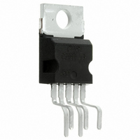
L4925 STMicroelectronics, L4925 Datasheet - Page 9

L4925
Manufacturer Part Number
L4925
Description
IC REG LDO 5V PENTAWATT
Manufacturer
STMicroelectronics
Datasheet
1.L4925PD013TR.pdf
(14 pages)
Specifications of L4925
Regulator Topology
Positive Fixed
Voltage - Output
5V
Voltage - Input
6 ~ 28 V
Voltage - Dropout (typical)
0.3V @ 500mA
Number Of Regulators
1
Current - Output
500mA
Current - Limit (min)
550mA
Operating Temperature
-40°C ~ 125°C
Mounting Type
Through Hole
Package / Case
Pentawatt-5 (Vertical, Bent and Staggered Leads)
Lead Free Status / RoHS Status
Contains lead / RoHS non-compliant
Other names
497-3911
Available stocks
Company
Part Number
Manufacturer
Quantity
Price
Part Number:
L4925
Manufacturer:
ST
Quantity:
20 000
Part Number:
L4925N
Manufacturer:
ST
Quantity:
20 000
Part Number:
L4925PD
Manufacturer:
ST
Quantity:
20 000
Company:
Part Number:
L4925PD-LF
Manufacturer:
TOSHIBA
Quantity:
375
Part Number:
L4925PD-LF
Manufacturer:
ST
Quantity:
20 000
Part Number:
L4925PD013TR
Manufacturer:
ST
Quantity:
20 000
L4925
3.2
Figure 4.
Figure 5.
Reset circuit
The block circuit diagram of the reset circuit is shown in
supervises the output voltage. The reset threshold of 4.5 V is defined with the internal
reference voltage and standby output divider. The reset pulse delay time t
the charge time of an external capacitor CT:
The reaction time of the reset circuit originates from the discharge time limitation of the reset
capacitor CT and it is proportional to the value of CT. The reaction time of the reset circuit
increases the noise immunity. Standby output voltage drops below the reset threshold only a
bit longer than the reaction time results in a shorter reset delay time.
The nominal reset delay time is generated for standby output voltage drops longer than
approximately 50 ms. The typical reset output waveforms are shown in
t
RD
=
C
-------------------
2μA
T
⋅
2V
Output voltage vs input voltage
Quiescent current vs supply voltage
Doc ID 1770 Rev 7
Figure
6. The reset circuit
Functional description
Figure
RD
, is defined with
7.
9/14


