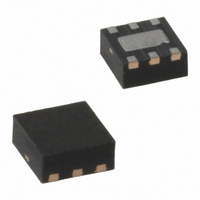
MIC5247-1.6BML TR Micrel Inc, MIC5247-1.6BML TR Datasheet - Page 8

MIC5247-1.6BML TR
Manufacturer Part Number
MIC5247-1.6BML TR
Description
IC REG LDO 150MA 1.6V 6-MLF
Manufacturer
Micrel Inc
Datasheet
1.MIC5247-1.8YM5_TR.pdf
(11 pages)
Specifications of MIC5247-1.6BML TR
Regulator Topology
Positive Fixed
Voltage - Output
1.6V
Voltage - Input
2.7 ~ 6 V
Voltage - Dropout (typical)
0.15V @ 150mA
Number Of Regulators
1
Current - Output
150mA
Current - Limit (min)
160mA
Operating Temperature
-40°C ~ 125°C
Mounting Type
Surface Mount
Package / Case
6-MLF®, QFN
Lead Free Status / RoHS Status
Contains lead / RoHS non-compliant
Other names
MIC5247-1.6BMLTR
MIC5247-1.6BMLTR
MIC5247-1.6BMLTR
MIC5247
Applications Information
Enable/Shutdown
The MIC5247 comes with an active-high enable pin that can
disable the regulator. Forcing the enable pin low disables the
regulator and sends it into a “zero” off-mode-current state.
In this state, current consumed by the regulator goes nearly
to zero. Forcing the enable pin high enables the output volt-
age. This part is CMOS and the enable pin cannot be left
floating; a floating enable pin may cause an indeterminate
state on the output.
Input Capacitor
An input capacitor is not required for stability. A 1µF input
capacitor is recommended when the bulk AC supply capaci-
tance is more than 10 inches away from the device, or when
the supply is a battery.
Output Capacitor
The MIC5247 requires an output capacitor for stability. The
design requires 1µF or greater on the output to maintain stabil-
ity. The capacitor can be a low-ESR ceramic chip capacitor.
The MIC5247 has been designed to work specifically with
low-cost, small chip capacitors. Tantalum capacitors can also
be used for improved capacitance over temperature. The
value of the capacitor can be increased without bound.
Bypass Capacitor
A capacitor can be placed from the noise bypass pin to ground
to reduce output voltage noise. The capacitor bypasses the
internal reference. A 0.01µF capacitor is recommended for
applications that require low-noise outputs.
The bypass capacitor can be increased without bound, further
reducing noise and improving PSRR. Turn-on time remains
constant with respect to bypass capacitance. Refer to the
“Typical Characteristics” section for a graph of turn-on time
vs. bypass capacitor.
Transient Response
The MIC5247 implements a unique output stage to dramati-
cally improve transient response recovery time. The output is
a totem-pole configuration with a P-Channel MOSFET pass
device and an N-Channel MOSFET clamp. The N-Channel
clamp is a significantly smaller device that prevents the output
voltage from overshooting when a heavy load is removed.
This feature helps to speed up the transient response by
significantly decreasing transient response recovery time
during the transition from heavy load (100mA) to light load
(85µA).
Active Shutdown
The MIC5247 also features an active shutdown clamp, which
is an N-Channel MOSFET that turns on when the device is
disabled. This allows the output capacitor and load to dis-
charge, de-energizing the load.
Thermal Considerations
The MIC5247 is designed to provide 150mA of continuous
current in a very small package. Maximum power dissipation
can be calculated based on the output current and the voltage
drop across the part. To determine the maximum power dis-
sipation of the package, use the junction-to-ambient thermal
M9999-022406
8
resistance of the device and the following basic equation:
T
125°C, and T
layout dependent; Table 1 shows examples of junction-to-
ambient thermal resistance for the MIC5247.
The actual power dissipation of the regulator circuit can be
determined using the equation:
Substituting P
conditions that are critical to the application will give the
maximum operating conditions for the regulator circuit. For
example, when operating the MIC5247-2.4BM5 at room
temperature with a minimum footprint layout, the maximum
input voltage for a set output current can be determined as
follows:
The junction-to-ambient thermal resistance for the minimum
footprint is 235°C/W, from Table 1. The maximum power dis-
sipation must not be exceeded for proper operation. Using
the output voltage of 2.4V and an output current of 150mA,
the maximum input voltage can be determined. Because this
device is CMOS and the ground current is typically 100µA over
the load range, the power dissipation contributed by the ground
current is < 1% and can be ignored for this calculation.
Therefore, a 2.4V application at 150mA of output current
can accept a maximum input voltage of 5.2V in a SOT-23-5
package. For a full discussion of heat sinking and thermal
effects on voltage regulators, refer to the “Regulator Ther-
mals” section of Micrel’s Designing with Low-Dropout Voltage
Regulators handbook.
Fixed Regulator Applications
Package
SOT-23-5 (M5)
J
Figure 1. Ultra-Low-Noise Fixed Voltage Application
(max) is the maximum junction temperature of the die,
P
425mW = (V
425mW = V
785mW = V
V
P max
P max
P max
D
D
D
D
IN
(
(
(
=
Table 1. SOT-23-5 Thermal Resistance
(max) = 5.2V
(
V
IN
)
)
)
A
=
=
=
D
−
is the ambient operating temperature. θ
(max) for P
V
425mW
V
125 C 25 C
IN
T max
OUT
θ
Minimum Footprint
IN
IN
J
JA
IN
235 C /W
(
MIC5247-x.xBM5
×150mA
×150mA – 360mW
° −
)
Recommended
θ
– 2.4V) 150mA
235°C/W
×
JA
°
1
2
3
I
)
OUT
−
T
D
°
A
+
and solving for the operating
V
IN
4
×
5
I
GND
0.01µF
θ
Copper Clad
JA
V
185°C/W
1µF
OU T
1” Square
February 2006
Micrel, Inc.
145°C/W
θ
JC
JA
is


