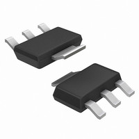
CS52015-1GSTR3 ON Semiconductor, CS52015-1GSTR3 Datasheet - Page 6

CS52015-1GSTR3
Manufacturer Part Number
CS52015-1GSTR3
Description
IC REG LIN 1.5A ADJ-OUT SOT223
Manufacturer
ON Semiconductor
Datasheet
1.CS52015-1GSTR3.pdf
(9 pages)
Specifications of CS52015-1GSTR3
Regulator Topology
Positive Adjustable
Voltage - Output
1.25 ~ 5.5 V
Voltage - Input
Up to 7V
Voltage - Dropout (typical)
1.05V @ 1.5A
Number Of Regulators
1
Current - Output
1.5A
Current - Limit (min)
1.6A
Operating Temperature
0°C ~ 70°C
Mounting Type
Surface Mount
Package / Case
SOT-223 (3 leads + Tab), SC-73, TO-261
Lead Free Status / RoHS Status
Contains lead / RoHS non-compliant
Other names
CS52015-1GSTR3OS
Protection Diodes
regulator it is sometimes necessary to add protection diodes.
If the input voltage of the regulator gets shorted, the output
capacitor will discharge into the output of the regulator. The
discharge current depends on the value of the capacitor, the
output voltage and the rate at which V
CS52015−1 linear regulator, the discharge path is through a
large junction and protection diodes are not usually needed.
If the regulator is used with large values of output
capacitance and the input voltage is instantaneously shorted
to ground, damage can occur. In this case, a diode connected
as shown in Figure 13 is recommended.
Output Voltage Sensing
possible to provide true remote load sensing. Load
regulation is limited by the resistance of the conductors
connecting the regulator to the load.
occurs when R1 is connected directly to the output pin of the
regulator as shown in Figure 14. If R1 is connected to the
load, RC is multiplied by the divider ratio and the effective
resistance between the regulator and the load becomes.
where R
V
IN
Figure 14. Grounding Scheme for Adjustable Output
When large external capacitors are used with a linear
Since the CS52015−1 is a three terminal regulator, it is not
For the adjustable regulator, the best load regulation
Regulator to Minimize Parasitic Resistance Effects
V
Figure 13. Protection Diode for Large Output
IN
C
= conductor parasitic resistance.
V
IN
CS52015−1
C
1
Adj
V
CS52015−1
IN
R C
IN4002 (Optional)
V
OUT
Capacitors
Adj
V
C
OUT
R1 ) R2
Adj
R1
R
R
1
2
R
C
Conductor Parasitic
R
R
IN
1
2
Resistance
drops. In the
C
V
2
OUT
http://onsemi.com
R
LOAD
6
Calculating Power Dissipation and Heat Sink
Requirements
shutdown and current limit circuitry to protect the device.
High power regulators such as these usually operate at high
junction temperatures so it is important to calculate the
power dissipation and junction temperatures accurately to
ensure that an adequate heat sink is used.
electrical isolation may be required for some applications.
Thermal compound should always be used with high current
regulators such as these.
following four factors:
1. Maximum Ambient Temperature T
2. Power dissipation P
3. Maximum junction temperature T
4. Thermal resistance junction to ambient R
dissipation are determined by the design while the
maximum junction temperature and the thermal resistance
depend on the manufacturer and the package type.
P D(max) + { V IN(max) * V OUT(min) } I OUT(max) ) V IN(max) I Q
where:
package to improve the flow of heat away from the IC and
into the surrounding air.
outside environment has a thermal resistance. Like series
electrical resistances, these resistances are summed to
determine R
junction and the surrounding air.
1. Thermal Resistance of the junction to case, R
2. Thermal Resistance of the case to Heat Sink, R
3. Thermal Resistance of the Heat Sink to the ambient
The CS52015−1 linear regulator includes thermal
The case is connected to V
The thermal characteristics of an IC depend on the
These four are related by the equation
The maximum ambient temperature and the power
The maximum power dissipation for a regulator is:
V
V
I
I
A heat sink effectively increases the surface area of the
Each material in the heat flow path between the IC and the
These are connected by the equation:
OUT(max)
Q
IN(max)
OUT(min)
application
(°C/W)
(°C/W)
air, R
is the maximum quiescent current at I
qSA
R QJA + R QJC ) R QCS ) R QSA
is the maximum input voltage,
qJA
is the minimum output voltage,
is the maximum output current, for the
(°C/W)
, the total thermal resistance between the
T J + T A ) P D
D
(Watts)
OUT
R QJA
on the CS52015−1,
J
A
(°C)
(°C)
OUT(max)
qJA
(°C/W)
qJC
qCS
.
(1)
(2)
(3)


